
Understanding Mixed Technology: Definitions, Core Drivers, and Industry Data
Turnkey mixed technology PCB fabrication is the synchronized manufacturing process of producing bare circuit boards and assembling both ultra-fine-pitch surface-mount devices (SMD) and mechanically anchored through-hole technology (THT) components on complex substrate architectures like rigid-flex and heavy copper. By combining bare-board fabrication with component sourcing and hybrid assembly under unified thermal modeling, end-to-end turnkey manufacturing eliminates thermal-mass delamination, barrel fill shortfalls, and yield fallout. Modern electronic hardware rarely lives purely in the digital domain. High-performance systems require high-density interconnect (HDI) microcontrollers, 0.4mm pitch BGAs, and 0201 passives to coexist alongside terminal blocks, high-current inductors, and chassis-grounded relays.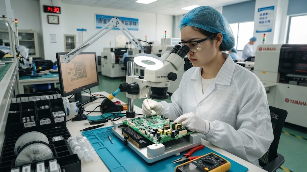
Mixed Technology PCB Assembly: A manufacturing methodology integrating surface mount technology (SMT) and plated through-hole (PTH) soldering on a single substrate, balancing microscopic coplanarity tolerances with macroscopic thermal absorption requirements.Data from empirical microsection analyses across complex product introductions indicates that over 42% of first-pass assembly failures on hybrid boards stem from thermal imbalance during reflow. When massive through-hole connectors absorb heat faster than surrounding copper planes, adjacent fine-pitch SMT solder joints suffer from incomplete wetting or severe solder balling. Deploying end-to-end turnkey PCB assembly services resolves this disparity by unifying substrate DFM with precision advanced SMT assembly lines and automated soldering processes.
Substrate Engineering: Rigid-Flex & Heavy Copper Stackup Interdependence
Fabricating bare boards that merge polyimide flex cores with heavy copper (3oz to 6oz+) rigid sections requires stringent lamination controls. Standard FR-4 parameters cause catastrophic delamination when subjected to the repeated thermal cycles of mixed assembly.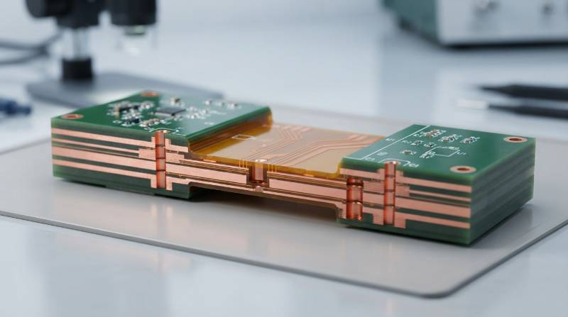
Resin Starvation and Prepreg Flow Dynamics
Heavy copper inner layers require customized prepreg selection. Etching 4oz copper leaves deep resin-void valleys between traces that standard 1080 or 2116 glass styles cannot fill.- High-Resin Content Prepregs: Use 106 or 1080 high-resin (HR) prepregs (resin content > 65%) combined with medium-flow bonding sheets to encapsulate thick copper foil edges.
- Etch Compensation: Account for an etch factor ratio of 2:1 or 3:1 on thick copper foil etching to avoid conductor necking.
- Transition Zone Radii: In rigid-flex designs per IPC-6013, maintain a minimum coverlay overlap of 1.0mm beyond the rigid transition line to mitigate mechanical sheer.
Engineering Insight: Dynamic bending radius guidelines must adhere strictly to IPC-2223 rules. For 1-2 layer flexible tails, maintain a bend radius of at least 10× flex thickness; for dynamic flex installations, maintain at least 20× to prevent polyimide coverlay delamination during convective reflow.
The Visianda EMS Mixed-Tech Integrity Protocol (MTIP™)
To overcome fabrication-to-assembly defect propagation, Visianda EMS developed a unified 5-stage framework applied to every turnkey hybrid NPI program.- Fabrication-Assembly Thermal Balancing: Simulation of localized copper plane densities to balance thermal absorption across high-mass THT pads and low-mass SMT pads.
- Keep-Out Geometry Verification: Automated 3D CAD collision validation for selective soldering nozzle sweeps and pallet edge clearances.
- Dynamic Dual-Zone Reflow Profiling: Multi-channel KIC thermal profiling targeting ±3°C tolerance windows across BGA junctions and connector body plastic thresholds.
- Hybrid Solder Joint Metallurgical Validation: Intermetallic compound (IMC) thickness verification (1.0µm to 3.0µm) via destructive microsectioning on initial production coupons.
- Unified Functional Stress Testing: Synchronous boundary-scan and high-current power distribution verification under loaded thermal imaging.
Soldering Technology Selection: Pin-in-Paste (PiP) vs. Selective Wave vs. Palletized Wave
Soldering through-hole components onto heavy copper assemblies cannot rely on universal bulk wave soldering. Component density on secondary sides requires targeted energy transfer.
| Soldering Parameter | Pin-in-Paste (Intrusive Reflow) | Automated Selective Soldering | Palletized Wave Soldering |
|---|---|---|---|
| Process Compatibility | High-temp through-hole components only (≥260°C for 10s) | Standard & high-mass THT components | High-mix legacy THT components |
| Thermal Stress on SMT | None (Standard single reflow cycle) | Extremely Low (Localized mini-wave) | Medium-High (Pallet pocket dependent) |
| Tooling / Fixture Cost | Low (Custom stencil apertures only) | Low-Medium (Software programming & nozzle) | High (CNC Durostone/Titanium pallets) |
| IPC-A-610 Class 3 Barrel Fill | Challenging on >1.6mm thick / 3oz+ boards | Consistently >75% to 100% vertical fill | High fill; risk of micro-bridging |
Comprehensive DFM & Keep-Out Rules for Mixed-Technology Assemblies
Design for Manufacturability (DFM) errors in mixed technology layouts lead to solder bridging, damaged components, or the need for manual hand-soldering.
Critical Clearances and Tolerances
- Selective Soldering Keep-Out: Maintain a minimum 3.0mm edge-to-edge clearance between THT pad rings and adjacent SMD pads. For deep nozzles (e.g., 6mm+ reach), increase clearance to 5.0mm.
- Drill-to-Copper Spacing: For 3oz-4oz heavy copper planes, maintain a minimum drill-to-copper distance of 14 mils (0.35mm) to prevent internal shorting during hole drilling.
- Thermal Relief Spoke Design: Connect THT ground pins to internal copper planes using 4-spoke thermal relief geometries. For a 4oz plane, spoke widths must be ≥0.5mm with a total cross-sectional area satisfying current capacity per IPC-2152.
- Pin-in-Paste Stencil Apertures: The solder paste volume must equal roughly 2.1× the volume of the unfilled PTH barrel plus the component pin volume. Employ step-up stencils (e.g., 150µm stepped to 200µm) or overprinted crosshatch stencils on non-wettable mask.
Thermal Management & High-Current Calculations (IPC-2152)
In high-power industrial and automotive electronics, mixed-technology boards manage heavy current switching next to sensitive sensor lines. IPC-2152 empirical formulas dictate trace geometry to prevent thermal runaway. The standard trace cross-sectional area calculation is:A = ( I / (k * ΔT^0.44) )^(1 / 0.725)Where I is current in Amperes, ΔT is permissible temperature rise in °C, and k is a derating constant (0.048 for external layers, 0.024 for internal layers).
High-Current Via Matrices and Isolation
Thermal via arrays beneath SMD power packages (such as D2PAK or TO-LL) must use 0.3mm drill diameters on a 0.65mm pitch grid. Via fill types (IPC-4761 Type VII epoxy plugged and capped) prevent solder robbing away from device pads. When engineering boards for automotive electronics manufacturing, creepage and clearance distances must strictly observe IEC 60664-1 pollution degree 2 ratings to prevent high-voltage arcing across heavy copper rail edges.Turnkey Sourcing & Supply Chain Risk Mitigation for Hybrid BOMs
Mixed technology Bills of Materials (BOMs) carry inherent supply chain friction: high-density SMT ICs follow short 18-month commercial lifecycles, whereas high-power THT connectors, inductors, and transformers operate on multi-year lifecycles with longer procurement lead times.Component Pedigree and Anti-Counterfeit Controls
- Dual-Track Sourcing: Visianda EMS maintains direct authorized manufacturer pipelines for active semiconductors alongside strategic stocking for specialized high-power magnetics.
- AS6174 Counterfeit Prevention: Incoming verification incorporates Decapsulation, X-Ray Fluorescence (XRF) for material composition, and automated optical die marking analysis.
- End-of-Life (EOL) Monitoring: Continuous BOM scrubbing identifies NRND (Not Recommended for New Designs) parts during early DFM review, preventing mid-lifecycle redesigns.
End-of-Line Quality Assurance: AOI, 3D AXI, Flying Probe, and ICT
Verifying joint integrity across mixed assemblies requires multi-axis inspection. While 3D AOI captures SMD coplanarity, it cannot confirm vertical solder climb through heavy copper barrels.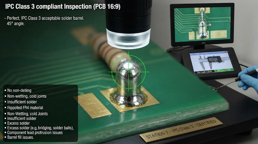
Inspection Regimes per IPC-A-610 Class 3
- 3D Automated X-ray Inspection (AXI): Measures circumferential through-hole barrel fill percentage. IPC-A-610 Class 3 mandates ≥75% vertical solder fill, which AXI computes algorithmically without destructive testing.
- In-Circuit Testing (ICT): Customized dual-stage bed-of-nails fixtures apply mechanical support for heavy boards to prevent micro-cracking solder balls beneath dense BGAs during test probe actuation.
- Flying Probe Testing: Deployed during NPI and small-batch runs to validate netlist integrity and passive component values without dedicated fixture delays.