
Understanding Ceramic PCB Substrates: Al2O3, AlN, and Si3N4
Ceramic PCB prototype fabrication delivers thermal conductivity ranging from 24 W/mK to over 230 W/mK, maintaining structural and electrical stability under continuous operating temperatures exceeding 300°C. By eliminating the organic resin matrix found in standard FR-4, ceramic substrates provide low dielectric loss (tan δ < 0.001) and matched coefficients of thermal expansion (CTE) with bare silicon and GaN power dies.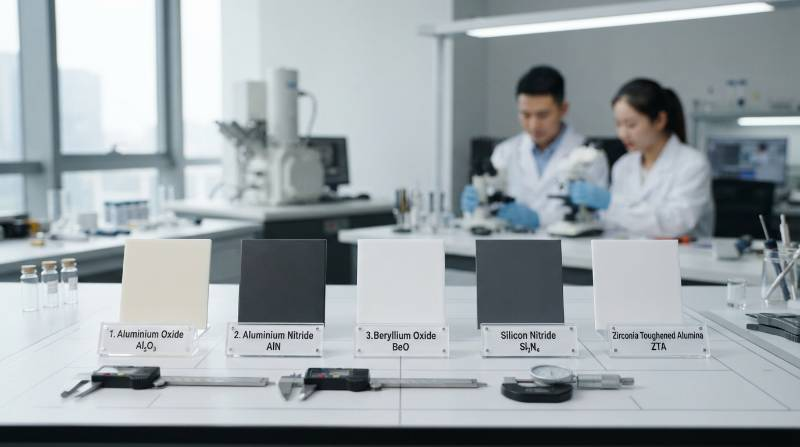
Thermal Conductivity (k-value): The rate at which heat transfers through a unit thickness of a material under a unit temperature gradient, measured in Watts per meter-Kelvin (W/mK).
| Material Property | Alumina (96% Al2O3) | Aluminum Nitride (AlN) | Silicon Nitride (Si3N4) |
|---|---|---|---|
| Thermal Conductivity (W/mK) | 24 – 28 | 170 – 230 | 80 – 90 |
| CTE (ppm/°C, 25–400°C) | 6.8 – 7.2 | 4.3 – 4.7 | 2.8 – 3.2 |
| Dielectric Constant (εr @ 1 GHz) | 9.6 – 9.8 | 8.6 – 8.9 | 8.1 – 8.3 |
| Dielectric Loss (tan δ @ 1 GHz) | < 0.0004 | < 0.0005 | < 0.0010 |
| Bending Strength (MPa) | 380 – 450 | 300 – 350 | 650 – 850 |
Key Metallization Technologies: DPC vs. DBC vs. AMB
Ceramics cannot be electroplated without an adhesion seed layer. Metallization method selection impacts prototype routing density, current density limits, and delivery speed for rapid prototype PCBA services.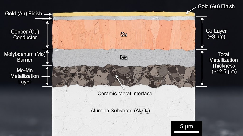
1. Direct Plated Copper (DPC)
DPC utilizes vacuum sputtering to apply a thin titanium adhesion layer and a copper seed film onto bare ceramic, followed by photolithography and standard electroplating. This thin-film technique produces sharp conductor traces with fine Line/Space (L/S) resolutions down to 20 µm / 20 µm. DPC is the ideal choice for high-frequency RF substrates, optoelectronic submounts, and tight-pitch multi-pad arrays.2. Direct Bonded Copper (DBC)
DBC bonds high-purity copper foil directly to Al2O3 or AlN substrates via a high-temperature eutectic melt (Cu-O eutectic at 1065°C). Copper cladding thicknesses range from 127 µm to 500 µm (4 oz to 14 oz), allowing continuous currents above 100A. DBC trace geometries require broader trace-and-space envelopes (≥ 150 µm / 150 µm) due to isotropic copper etching profiles.3. Active Metal Brazing (AMB)
AMB applies a reactive brazing alloy paste (typically Ag-Cu-Ti) under vacuum at ~800°C to secure heavy copper foils to high-toughness Silicon Nitride (Si3N4) substrates. AMB boards withstand over 5,000 thermal shock cycles (-40°C to 150°C), making them the primary solution for traction inverters and aviation power distributions.Precision Laser Drilling, Scribing, and Edge Profiling
Mechanical CNC routing easily shatters brittle ceramic tiles. Therefore, ceramic micro-vias, castellations, and singulation boundaries must be produced using specialized laser processing systems.- Ultraviolet (UV 355 nm) Lasers: Provide cold laser micro-machining with spot sizes down to 15 µm, ideal for precise blind micro-vias and clean DPC edge trenches without heat-affected zones (HAZ).
- CO2 Laser Pulse Scribing: Utilized for fast through-wafer perforations and breakout snap-lines. Hole pitches are kept at ≥ 1.5× substrate thickness to prevent micro-fracture propagation along the web.
- Diamond Saw Dicing: Applied for final rectilinear singulation to maintain edge dimensional tolerances within ±0.05 mm and prevent micro-chipping along metalized outer margins.
The Visianda EMS Ceramic Precision Prototyping Framework (CPPF)
To eliminate scrap risk and reduce fast-turn turnaround from weeks to days, Visianda EMS operates under the proprietary Ceramic Precision Prototyping Framework (CPPF). This 4-stage engineering protocol ensures direct transitions from CAM data to functional, zero-defect assemblies under complete turnkey PCB assembly management.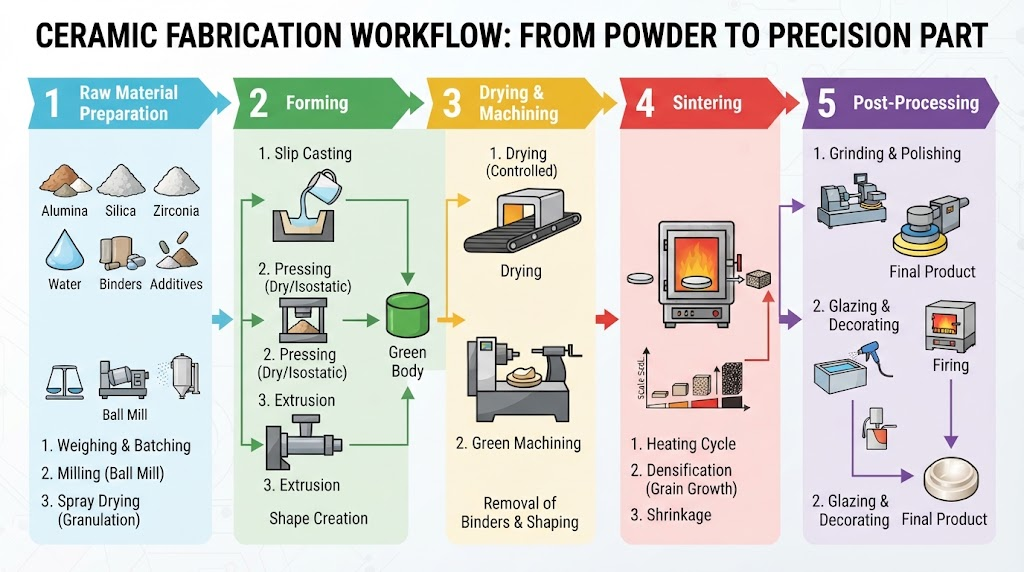
- Stage 1: Multi-Physics CTE & Thermal Simulation We run finite element analysis (FEA) on the raw CAD package to evaluate localized stress points between bare semiconductor dies, thick copper layers, and the ceramic core. Copper balances are optimized across top and bottom layers to prevent tile warpage during high-temperature processing.
- Stage 2: Micro-Ablation & Dynamic Laser Calibrations Substrate laser machining profiles dynamically adjust laser dwell time and pulse repetition rates according to actual ceramic batch density. We verify ceramic surfaces under 3D optical profilometry to ensure surface roughness (Ra) remains between 0.3 µm and 0.5 µm for optimal film adhesion.
- Stage 3: Controlled-Atmosphere SMT Vacuum Reflow Populated ceramic prototypes pass through multi-zone reflow systems with inert Nitrogen (N2) blanketing (< 50 ppm O2) and dynamic vacuum extraction (< 10 mbar) to eliminate under-pad flux entrapment and minimize void formation.
- Stage 4: Multi-Axis Acoustic & 3D X-Ray Non-Destructive Screening Every fabricated ceramic unit undergoes non-destructive evaluation. Scanning Acoustic Microscopy (C-SAM) detects sub-surface copper delamination, while high-resolution 3D X-ray systems verify solder coverage, ensuring full IPC-6012DS Class 3/A aerospace compliance.
Prototyping DFM: Thermal Profiles, Void Minimization, and Assembly
Ceramic boards behave differently than standard polyimide or FR-4 substrates during SMT component placement and soldering. Their high thermal conductivity pulls thermal energy directly away from the solder joints, requiring custom thermal profile engineering during precision SMT assembly.
Reflow Profile Optimization and Micro-Cracking Avoidance
Standard rapid ramp rates cause severe mechanical shock in crystalline ceramic cores. We maintain heating ramp rates strictly below 1.5°C/second and cooling rates below 2.0°C/second to minimize internal crystal lattice shear strain. In our manufacturing experience, failing to pre-heat ceramic assemblies uniformly across a bottom-side hot-plate zone before localized rework will instantly initiate micro-fractures along nearby laser-cut vias.Void Minimization Under High-Power Components
Solder voiding under high-current MOSFETs, GaN FETs, and laser diode chips degrades the thermal stack-up. Uncontrolled voiding (> 25%) creates hot spots, accelerating semiconductor failure.- Vacuum Soldering: Applying vacuum assist during solder liquidus stages pulls out gaseous flux residues, reliably driving solder void ratios below 5% in accordance with MIL-STD-883 Method 2012 requirements.
- Solder Preforms with Integrated Flux: Precise robotic placement of exact-volume Au80Sn20 or SAC305 preforms eliminates paste spatter on bare DPC traces.
- Surface Finish Compatibility: Electroless Nickel Electroless Palladium Immersion Gold (ENEPIG) finishes provide corrosion resistance, excellent solder wettability, and reliable wire-bonding attachment for pure gold (Au) and aluminum (Al) wire wedges.
High-Reliability Applications: Automotive, RF, and Power Systems
Ceramic PCB prototypes validate electrical and thermal margins in demanding real-world environments before volume tooling investments occur, particularly in automotive electronics manufacturing.- Electric Vehicle (EV) Power Inverters: Direct Bonded Copper on AlN cores handles severe power-switching cycles in 800V silicon-carbide (SiC) dual inverters, keeping gate driver operating temperatures balanced.
- Automotive Solid-State LiDAR: High thermal dissipation DPC Alumina submounts support high-pulse multi-channel pulsed laser diodes with tight line placement tolerances.
- RF & Microwave Transceivers: Ka-band and millimeter-wave communication front-ends rely on Al2O3 DPC circuits for stable dielectric constants through 40+ GHz and minimal transmission line losses.
- Industrial High-Lumen Chip-on-Board (COB) LEDs: Fast-turn Alumina boards quickly vent heat from high-density emitter arrays to eliminate chromaticity drift and lumen degradation.
Cost Drivers and Rapid Lead-Time Compression (24 to 72 Hours)
Accelerating ceramic fabrication prototypes while managing project costs requires careful optimization of several manufacturing factors:- Raw Substrate Selection: Standard 96% Al2O3 offers the most economical pricing. Reserve AlN and Si3N4 for assemblies with strict dissipation requirements or high flexural stress environments.
- Layer Count and Metallization Complexity: Single-sided and double-sided DPC boards maintain faster throughput times than complex multi-layer High-Temperature Co-Fired Ceramic (HTCC) or Low-Temperature Co-Fired Ceramic (LTCC) modules.
- Pre-Tooled Stock Tile Geometry: Standardizing prototype layouts to fit standard ceramic master master sheets (e.g., 4.5" x 4.5" or 5.0" x 7.0") eliminates custom tooling setups.
- Streamlined SMT Transitions: Utilizing Visianda EMS’s integrated substrate fab and high-speed automated SMT lines cuts assembly hand-off intervals, achieving complete turnkey prototype turnarounds within 24 to 72 hours.