
Visianda manufactures rigid-flex PCBs that combine the component-mounting capability of rigid boards with the routing flexibility of FPC. Our rigid-flex designs eliminate inter-board connectors, reduce assembly steps, and enable packaging geometries impossible with separate rigid boards and cables.
What Is a Rigid-Flex PCB?
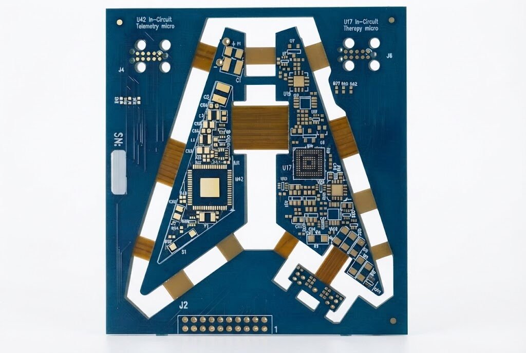
A rigid-flex PCB integrates rigid FR4 sections and flexible polyimide sections into a single laminated structure. Components are mounted on the rigid sections, while the flexible sections route signals between them — replacing connectors and wire harnesses with a single integrated circuit.
The key advantage of rigid-flex over separate rigid boards connected by FPC cables is reliability: there are no connector contacts to corrode, loosen, or mismate. The flex section is a continuous copper trace, not a separable connection. This is why rigid-flex is the preferred interconnect technology for aerospace, medical implants, and military electronics.
Visianda's rigid-flex process uses polyimide flex layers laminated with FR4 rigid layers in a single pressing operation. The flex zones are defined by selective removal of the rigid layers, leaving only the flexible polyimide and copper layers in the bend areas.
Technical Specifications
Key Advantages
Eliminates Connectors
Replaces inter-board connectors with continuous copper traces — eliminating the most common failure point in electronic assemblies.
3D Packaging
Fold the rigid sections into a three-dimensional configuration, fitting complex electronics into tight enclosures.
Weight & Space Reduction
Eliminates connectors, cables, and their associated mounting hardware — reducing weight by 30–70% vs. equivalent multi-board assemblies.
Improved Reliability
No connector contacts to corrode or loosen. Preferred for aerospace, medical implants, and military applications.
Reduced Assembly Steps
Single assembly operation vs. multiple boards + cable assembly + connector mating — reducing labor cost and assembly errors.
Dynamic Flex Capability
Flex sections can be designed for millions of flex cycles for applications with moving parts or repeated folding.
Where It's Used
Medical Devices
Implantable devices, endoscopes, hearing aids
Aerospace
Avionics, satellite payloads, UAV electronics
Consumer Electronics
Foldable phones, laptops, cameras
Wearables
Smartwatches, AR/VR headsets, fitness devices
Military
Ruggedized electronics, body-worn systems
Industrial
Robotic arms, inspection cameras
Automotive
Dashboard electronics, steering controls
IoT
Compact sensor nodes, smart home devices
Why Choose Visianda for Rigid-Flex PCB?
- Rigid-flex DFM expertise — we review bend zone design, via placement, and stackup before production
- Minimum order from 5 pieces for prototype rigid-flex boards
- Full turnkey service: rigid-flex fabrication + SMT assembly in one order
- IPC-6013 inspection standards for rigid-flex PCBs
- 3D assembly simulation available to verify fit before production
- Experience with medical, aerospace, and military rigid-flex applications
Frequently Asked Questions
How do I design the bend zone for a rigid-flex PCB?
The bend zone should have no vias, no component pads, and traces routed perpendicular to the bend axis. Trace width in the flex zone should be increased by 20% compared to rigid sections to account for the higher stress. Our DFM team will review your bend zone design and flag any issues before production.
What is the minimum bend radius for rigid-flex?
For static applications (bent once during assembly), the minimum bend radius is 6× the total flex thickness. For dynamic applications (repeated flexing), we recommend 10× minimum. We can calculate the exact minimum bend radius for your specific stackup.
Can you assemble components on rigid-flex boards?
Yes. We assemble SMT components on the rigid sections of rigid-flex boards using standard reflow soldering. The flex sections are protected during assembly using custom fixtures. We do not place components in the flex zones.
How do you handle the rigid-to-flex transition zone?
The transition zone is a critical area where stress concentrates during bending. We add a coverlay extension of 0.3–0.5mm beyond the rigid section edge, and we recommend a teardrop or fillet at trace entry points into the flex zone. Our DFM report will include specific recommendations for your design.
Related PCB & PCBA Types
8-Layer Rigid-Flex for an Active Implantable Neural Stimulator
A US-based medical device company developing an active implantable neural stimulator for chronic pain management — requiring a rigid-flex PCB that folds into a 28mm × 18mm × 6mm titanium enclosure.
The Problem
The customer's design required an 8-layer rigid-flex with three rigid sections connected by two flex sections, all folding into a 3D configuration inside a hermetically sealed titanium can. The previous supplier's rigid-flex boards showed delamination at the rigid-to-flex transition zone after 500 thermal cycles (-40°C to +85°C), which is the sterilization and implant temperature range.
Key Challenges
- 8-layer stackup: 4 rigid layers + 2 flex layers + 2 coverlay layers, total thickness 0.8mm in rigid zones
- Flex zone width only 4mm — requiring 0.075mm trace width at 0.075mm spacing
- 500 thermal cycles -40°C to +85°C without delamination (ISO 10993 implant requirement)
- Blind vias in rigid sections for BGA breakout on a Texas Instruments MSP430 microcontroller
- ISO 13485 process documentation for Class III implantable device regulatory submission
Our Solution
We redesigned the rigid-to-flex transition zone with a 0.5mm coverlay overlap and added a 25μm PI stiffener transition layer to distribute the CTE mismatch stress between the FR4 rigid section (CTE 14 ppm/°C) and the PI flex section (CTE 20 ppm/°C). The lamination cycle was modified to use a lower peak temperature (175°C vs. standard 185°C) with extended dwell time to minimize residual stress in the transition zone. All flex zone traces were routed with 20% wider width than the minimum and with teardrop entries at pad connections. The complete process was documented in an IQ/OQ/PQ validation package including 10 boards subjected to 1000 thermal cycles for process qualification.
Results & Outcomes
"This was the most demanding rigid-flex project we've attempted, and Visianda was the only supplier willing to take on the process qualification work. The validation package they delivered was accepted by our notified body without any requests for additional data."
Principal Engineer, Medical Device Company — Minneapolis, MN, USA