
Core Cost Drivers in Prototype PCB Fabrication and Assembly
A reliable prototype pcb assembly cost estimator accounts for engineering setup (NRE), raw circuit board fabrication parameters, component bill of materials (BOM), and surface mount technology (SMT) machine placement time. For low-volume prototyping (5 to 50 units), initial setup and tooling fees constitute up to 45% to 60% of total project costs, while unit component procurement and fabrication scale proportionally with layer count, board material, and packaging density. Navigating the transition from CAD layout to physical hardware requires understanding how specific design choices drive manufacturing expenses. Selecting the right prototype PCBA services early in development helps teams prevent budget overruns during New Product Introduction (NPI).
1. Layer Count and Substrate Dielectrics
Bare board fabrication costs increase non-linearly with layer count. Transitioning from a standard 4-layer FR-4 board to an 8-layer HDI board with microvias often increases bare PCB raw fabrication expenses by 80% to 140% due to repeated lamination cycles, sequential laser drilling, and plating processes. High-frequency laminates such as Rogers RO4350B or PTFE substrates command a 300% to 500% material price premium over standard Tg150/Tg170 FR-4. Hybrid stackups—bonding Rogers layers to standard FR-4 cores—offer a cost-balanced solution for RF and high-speed analog prototypes.2. Surface Finish and Copper Thickness
Surface finish selection directly impacts component solderability and fine-pitch assembly yield:- HASL (Lead-Free): Lowest cost, but poor coplanarity makes it unsuitable for BGAs and 0.4mm pitch QFNs.
- ENIG (Electroless Nickel Immersion Gold): Flat planarity ideal for fine-pitch Surface Mount Devices (SMD); adds roughly 10% to 18% to bare board fabrication costs compared to HASL.
- ENEPIG / Immersion Silver: Higher cost, reserved for specialized high-density interconnects, wire-bonding, or critical aerospace applications.
3. SMT Placement Density and Component Geometry
Pick-and-place setup fees depend on the number of unique line items on your BOM rather than total component count. Setting up 45 unique part reels takes significantly more operator time than placing 200 instances of the same passive component. Fine-pitch ball grid arrays (BGA < 0.5mm pitch), ultra-dense 01005 passives, and complex leadless quad-flat no-leads (QFN) require slower feeder indexing, optical vision validation, and post-reflow automated X-ray inspection (AXI), slightly elevating placement labor rates.Hidden Prototype Expenses: Attrition, Packaging Surcharges, and MSD Baking
Online cost estimators frequently calculate component costs purely from single-unit distributor catalog pricing. In physical manufacturing, real production dynamics introduce secondary cost variables that must be factored into every early prototype build.
Component Attrition Rule: Automated high-speed SMT pick-and-place feeders require leader/trailer tape scrap margins. For passives in 0201 and 0402 packages, standard EMS feeder attrition rates require an overage buffer of 15% to 20% (or a minimum of 50–100 extra pieces) per line item.
Packaging Format: Cut-Tape vs. Continuous Reels
When purchasing 10 units of an IC packaged in cut tape, pick-and-place machines cannot automatically feed the strip without attaching custom leader tape or manually loading parts into specialized matrix trays. This manual handling adds loader surcharges or slows feeder cycling. Opting for "Digi-Reel" or factory mini-reels adds small repackaging fees per part, but drastically speeds up high-speed automated assembly while protecting sensitive IC leads from electrostatic discharge (ESD) and mechanical damage.Moisture-Sensitive Device (MSD) Baking and Environmental Controls
Components classified as Moisture Sensitivity Level (MSL) 3, 4, or 5 under the J-STD-033 Standard that arrive unsealed or exceed their floor-life window cannot undergo immediate reflow soldering. Moisture trapped inside plastic IC molds vaporizes at 245°C–260°C lead-free peak temperatures, causing internal delamination or package "popcorning". De-baking these components in temperature-controlled dry ovens for 24 to 48 hours at 125°C restores integrity before placement, but introduces scheduling delays and minor thermal handling overhead if inventory handling protocols are neglected during parts intake.Assembly Methodologies: Surface Mount, Through-Hole, and Mixed Technology
Assembly methodology directly influences production line configuration, cycle duration, and thermal profiling costs. Balancing SMT and Through-Hole Technology (THT) is a critical step in Design for Assembly (DFA) optimization.
| Assembly Process | Tooling & Setup NRE | Cycle Time Efficiency | Primary Cost Drivers |
|---|---|---|---|
| Single-Sided SMT | Low (Single Stencil) | Very Fast (Automated) | Feeder count, total component joints |
| Double-Sided SMT | Moderate (2 Stencils, 2 Runs) | Fast (Dual Reflow Cycles) | Secondary reflow profile, bottom-side glue/support |
| Selective Soldering (THT) | Moderate (Nozzle Programming) | Moderate | Thermal clearance keep-outs, cycle programming |
| Manual Hand Soldering | Very Low (Zero Tooling) | Slow (Operator Dependent) | Skilled manual touch labor per joint |
Turnkey vs. Consigned Assembly: Total Cost of Ownership Comparison
A frequent dilemma during NPI planning is whether to provide components to the assembler (consigned/kitted) or leverage the manufacturing partner's supply chain network (full turnkey).Consigned / Kitted Model Realities
While consigning parts appears cheaper on paper, it introduces non-obvious overhead: internal engineering hours spent placing 30+ separate purchase orders across distributors, receiving inspections, counting loose cut-tape, manual kitting, and repackaging for shipment to the EMS. If passive shortages or shipping delays occur, the assembly line sits idle—incurring line stoppage fees or missing project delivery milestones.Full Turnkey Total Cost Efficiency
Choosing full turnkey PCB assembly eliminates these administrative bottlenecks. EMS partners purchase directly through authorized volume distribution channels, securing wholesale pricing, consolidated shipping, and automated inventory checking against bill-of-materials revisions. Any scrap generated during feeder setup is absorbed and managed under the turnkey service level agreement, ensuring complete accountability from bare substrate fabrication to final board testing.Prototype Electrical Testing & Inspection Cost Matrix
Defect detection during prototyping prevents dead-on-arrival (DOA) boards from reaching firmware and validation engineers, where debugging unverified hardware can consume hundreds of engineering hours.Inspection Standard Compliance: Quality prototype builds adhere strictly to the IPC-A-610 Standard (Class 2 for commercial electronics; Class 3 for mission-critical and medical equipment), establishing verifiable acceptance criteria for solder fillets, voiding, and alignment.
Inspection Method Trade-offs
- Automated Optical Inspection (AOI): Standard on all modern SMT lines. Verifies component presence, polarity, correct markings, skew, and solder bridging. Low NRE, near-zero marginal cycle cost.
- 3D Automated X-ray Inspection (AXI): Essential for non-visible solder joints beneath BGAs, Land Grid Arrays (LGAs), and bottom-terminated QFN thermal pads. Quantifies solder voiding percentages to ensure compliance with IPC standards (< 25% voiding limit).
- Flying Probe Testing: Highly economical for low-volume prototypes (5 to 30 boards). Movable precision test needles check for nets, opens, shorts, and passive component values directly from CAD data without requiring expensive physical test fixtures ("bed-of-nails").
- Functional Circuit Testing (FCT): Validates board power-up sequences, firmware flashing, and I/O communication. Requires custom test harnesses or bench equipment, adding setup time but ensuring 100% functional readiness.
The Visianda 4-Stage Prototype Cost & DFM Optimization Protocol
To minimize pricing volatility, reduce line delays, and deliver rapid turnaround times, Visianda EMS utilizes an engineering-driven production framework built specifically for prototype-to-volume manufacturing.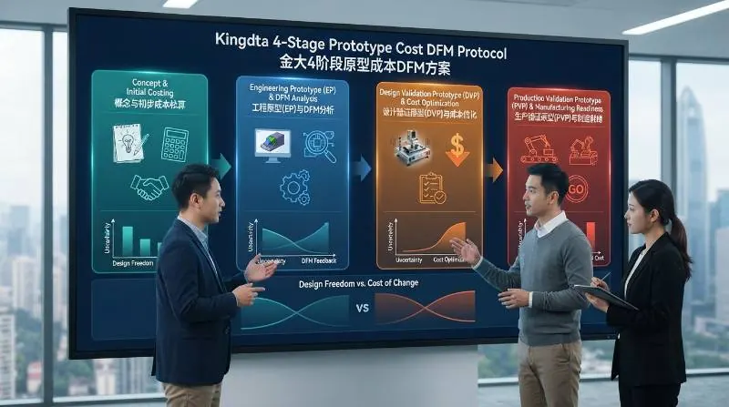
Stage 1: Pre-Layout BOM Health & Lifecycle Audit
Before releasing your Gerber files, our engineering team scrubs the BOM against global supply databases. We identify End-of-Life (EOL), Not Recommended for New Designs (NRND), and long lead-time components, recommending active, pin-compatible alternates to avoid costly board respins after fabrication.Stage 2: Comprehensive DFM/DFA Clearance Check
Our process engineers conduct a multi-point automated check across your layout. We verify annular rings, aspect ratios, solder mask dams (minimum 3–4 mil), component-to-edge clearances, and package footprints to eliminate solder bridging or tombstoning risks during reflow.Stage 3: Standardized Stencil & Panelization Optimization
We optimize custom laser-cut electropolished stencils, applying custom aperture reductions (e.g., window-pane patterns on QFN exposed pads) to control solder volume precisely. Panel design incorporates standardized fiducials, tooling holes, and mouse-bites/V-scores to maximize SMT rail efficiency and reduce mechanical stress during depanelization.Stage 4: Seamless Ramp-to-Volume Tooling Amortization
Data gathered during the prototype run—including reflow thermal profiles, machine placement coordinates, and automated inspection logs—is archived directly in our manufacturing execution system. When you scale from 10 prototypes to 10,000 production units, tooling and programming setup time is seamlessly amortized without redundant NRE charges.Complete RFQ Package Checklist for Instant Quoting Accuracy
Incomplete engineering data is the leading cause of quote delays and pricing revisions. When you request a prototype PCBA quote, submitting a complete documentation package guarantees rapid turnaround and fixed pricing.Mandatory RFQ Package Files
- Production Gerber Files (RS-274X or ODB++): Complete layer set including copper layers, solder mask, silkscreen, solder paste apertures, drill files (Excellon format), and mechanical board outline.
- Structured Bill of Materials (.XLSX or .CSV): Must include distinct columns for:
- Reference Designators (e.g., C1, R3, U5)
- Quantity per board
- Manufacturer Name
- Full Manufacturer Part Number (MPN)
- Component Description / Value / Tolerance / Voltage
- Package / Footprint (e.g., 0603, SOIC-8, QFN-32)
- Component Type (SMD vs. THT vs. DNP / Do Not Populate)
- Centroid / Pick-and-Place File (XY Coordinates): Text or CSV file specifying reference designator, X-position, Y-position, rotation (0°–360°), and board side (Top or Bottom).
- Fabrication & Assembly Notes Drawing: Specification document noting board thickness (e.g., 1.6mm ± 10%), material type (FR-4 Tg170), copper weight, solder mask color, silkscreen color, surface finish (ENIG/HASL), and IPC inspection class requirements.
- Schematic & Special Handling Guidelines: Include any custom programming, potting, conformal coating, or serialization requirements.
Frequently Asked Questions
What is the standard turnaround time for quick-turn prototype PCB assembly?
Standard turnkey prototype turnaround typically ranges from 5 to 8 business days once components arrive. For mission-critical design iterations, expedited 24-hour to 48-hour quick-turn assembly options are available when all BOM components are in stock and engineering data is fully verified.What specific items make up Non-Recurring Engineering (NRE) charges?
NRE costs cover the fixed physical and digital setup required before automated production begins. This includes laser-cut SMT solder paste stencils, pick-and-place coordinate programming, bare-board phototooling/drilling setup, reflow oven thermal profiling, and optical inspection camera programming.Is there a Minimum Order Quantity (MOQ) for prototype PCBA services?
No. Visianda EMS supports prototype runs starting from just 1 to 5 boards. However, due to fixed NRE tooling and setup fees, assembling 10 to 25 boards typically yields a substantially lower per-unit cost than assembling a single board.How does Visianda EMS handle unexpected component shortages or obsolete parts?
During the initial BOM review, our engineering team cross-references component lifecycle databases. If a part is obsolete or has an extended lead time, we proactively suggest drop-in pin-compatible alternates or passive tolerance equivalents for customer engineering approval before placing orders.Accelerate Your Hardware Development with Visianda EMS
Eliminate quoting delays, avoid hidden component surcharges, and ensure first-pass prototype success. Leverage our comprehensive DFM analysis and reliable turnkey manufacturing capabilities for your next PCBA build.