
Any-Layer HDI PCB Microvia Laser Drilling: Technical Definition and Core Architecture
Evaluating an any-layer HDI PCB microvia laser drilling manufacturer requires auditing their laser beam optics, electroplating superfill chemistry, and layer-to-layer registration accuracy. High-yield Every-Layer Interconnect (ELIC) manufacturing demands sub-75µm microvias drilled with positional tolerances tighter than ±10µm and solid copper fills with less than 5µm dimpling. Any-Layer High-Density Interconnect (Any-Layer HDI), also designated as Every-Layer Interconnect (ELIC), removes the traditional glass-core substrate constraint found in standard multilayers. Instead of routing through-holes from outer surfaces, designers place stacked or staggered blind microvias across every individual dielectric layer. Mechanical drilling encounters extreme physical limits below 150µm (0.006 in). Drill bit deflection, tool breakage, and runout cause severe pad breakout on dense pitches. Laser ablation completely replaces mechanical bits to form microvias ranging from 50µm to 100µm in diameter. By routing through solid copper-filled microvias directly beneath component lands, ELIC architectures free up to 40% more routing area. This interconnect density is essential for 0.35mm pitch ultra-fine BGAs, advanced System-in-Package (SiP) modules, and compact mission-critical hardware.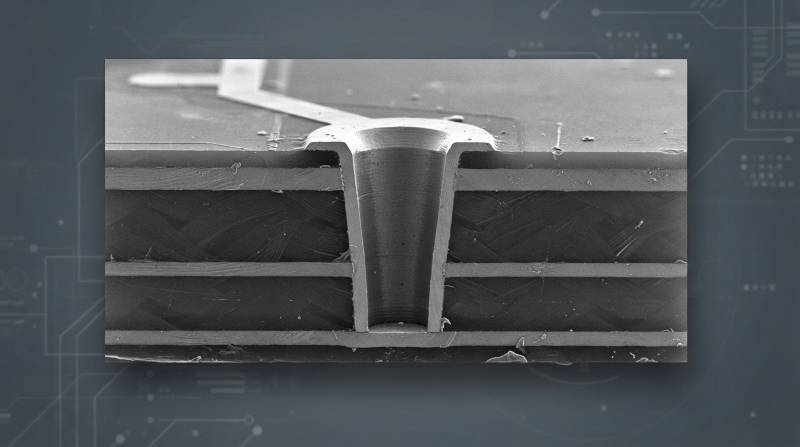
Core Engineering Data: Baseline Tolerances and Fabrication Metrics
Evaluating a board house requires benchmarking their baseline capabilities against production-grade ELIC HDI tolerances. Suppliers operating at the edge of capability without dedicated process controls introduce significant yield fall-out during assembly.| Process Parameter | Standard HDI (Type I-III) | Advanced Any-Layer ELIC | Visianda EMS Production Limit |
|---|---|---|---|
| Laser Microvia Diameter | 100µm – 125µm | 65µm – 75µm | 50µm (UV Laser direct) |
| Dielectric Layer Thickness | 60µm – 100µm | 35µm – 50µm | 25µm – 40µm |
| Target Aspect Ratio (Depth:Width) | 0.6:1 – 0.7:1 | 0.75:1 – 0.8:1 | 0.8:1 Controlled |
| LDI Alignment Registration | ±25µm | ±12.5µm | ±8µm Dynamic Scaling |
| Max Sequential Laminations | 2 – 3 Cycles | 5 – 6 Cycles | Up to 10 Cycles (ELIC) |
| Max Dimple Depth After Plating | < 15µm | < 7µm | ≤ 5µm Guaranteed |
Laser Drilling Mechanics: UV Photochemical vs. CO2 Photothermal Ablation
Laser drilling precision is determined by the optical physics of the laser source and how that wavelength interacts with copper foil and reinforced dielectric matrices.CO2 Laser Ablation (Infrared: 9.4µm to 10.6µm)
Pulsed CO2 lasers operate primarily via photothermal ablation. The infrared energy is intensely absorbed by resin systems and glass cloth, vaporizing the dielectric in microsecond bursts. However, bare copper reflects infrared wavelengths at rates exceeding 95%. Manufacturers using CO2 systems must either pre-etch copper windows via chemical lithography (conformal mask process) or treat the copper surface with black oxide chemistry to enhance absorption. Thermal dissipation during CO2 pulsing can create a wider Heat-Affected Zone (HAZ). If poorly controlled, this causes resin recession, glass bundle undercut, and barrel taper angles below 70 degrees.UV Laser Ablation (Ultraviolet: 355nm Third-Harmonic Nd:YAG)
UV lasers operate via photochemical ablation (cold ablation). High-energy UV photons directly break chemical bonds in both organic resin matrices and metallic copper lattices without generating excessive heat. This allows single-pass direct copper ablation (DCA) through top foil, dielectric, and stops cleanly on the inner capture pad. UV systems drill precise sub-65µm microvias with clean, near-vertical side walls (80° to 85° taper) and zero carbonization. The trade-off is throughput. UV drilling is significantly slower than CO2 ablation. Leading tier-1 manufacturers deploy hybrid laser systems: UV lasers cut the top copper foil with surgical precision, while high-speed CO2 heads instantly ablate the bulk dielectric core.Microvia Fill and Metallization Integrity: Plating Chemistry and Void Elimination
Ablating the blind hole is only half the engineering challenge. Solid copper metallization dictates whether stacked microvias survive multi-cycle assembly reflow.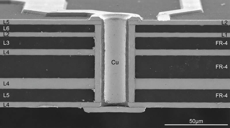
- Suppressors (Polymers): High molecular weight agents that adsorb onto high-current-density outer pad surfaces, suppressing planar copper deposition.
- Accelerators (Brighteners): Low molecular weight sulfur compounds that concentrate at the microvia bottom, accelerating localized copper growth.
- Levelers: Positively charged components that selectively migrate to microvia shoulders, preventing premature pinch-off and interior void formation.
Thermal-Mechanical Stress Across Multi-Cycle Sequential Laminations
Fabricating a 10-layer or 12-layer ELIC board requires 5 to 6 distinct sequential lamination cycles. Each cycle subjects the core stack to 190°C–220°C temperatures and hundreds of PSI of hydrostatic press pressure. This cumulative thermal exposure degrades resin cross-linking and degrades glass transition temperatures (Tg). Substrate materials for any-layer builds must feature low z-axis coefficients of thermal expansion (CTE < 40 ppm/°C below Tg) and decomposition temperatures (Td) exceeding 350°C. Standard FR-4 materials fail rapidly under these stresses. Any-layer stacks require specialized high-Tg (Tg ≥ 170°C–180°C) phenolic-cured modified epoxies, PPE/PPO, or polyimide systems, especially for harsh environments like automotive electronics assembly.The Visianda EMS HDI-PCBA Interconnect Qualification Protocol (IQ-Protocol)
To eliminate interface disconnects between bare-board laser drilling houses and SMT assembly lines, Visianda EMS operates under our proprietary four-phase engineering framework: The Visianda Interconnect Qualification Protocol (IQ-Protocol).
- Phase 1: Dynamic LDI-to-Laser Registration Calibration We verify supplier compensation algorithms for substrate non-linear dimensional movement. Substrates shrink and stretch during sequential press cycles; laser targeting must use localized fiducials per quadrant to maintain misregistration below ±10µm.
- Phase 2: Microsection & Metallurgical IST Coupon Validation Coupon microsections are analyzed on every panel. We inspect microvia barrel thickness, verify zero target-pad separation, and test for copper crystal structure purity via cross-polarized metallurgical imaging.
- Phase 3: DFM-to-DFA Synergy & Topography Mapping Prior to assembly, board topographies undergo non-contact laser surface profilometry. Outer via-in-pad dimples are checked to ensure coplanarity deviations remain strictly under 5µm across 0.35mm BGA footprints.
- Phase 4: In-line 3D AXI & Thermal Cycling Telemetry Post-reflow assemblies undergo 3D High-Resolution Automated X-ray Inspection (AXI) to map solder void distributions and verify interconnect integrity beneath ultra-dense arrays.
Downstream SMT Yield Impact: Preventing Micro-BGA Defects and Voiding
Bare-board HDI defects do not remain isolated; they transfer directly into the Surface Mount Technology line as component assembly failures. Microvia defects are the root cause of the majority of fine-pitch BGA assembly fallout.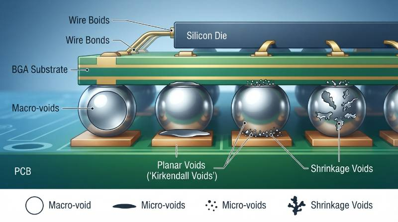
Supplier Evaluation Scorecard: Auditing Any-Layer HDI Board Houses
Use this weighted scorecard during on-site supplier audits to evaluate an any-layer HDI manufacturer's technical readiness and process capability.| Audit Category | Critical Verification Checklist | Weight | Minimum Pass |
|---|---|---|---|
| Laser Drilling Technology | Multi-head UV/CO2 platforms (Mitsubishi, ESI, Via Mechanics); optical auto-alignment; real-time beam pulse power monitoring; depth control accuracy ≤ ±2µm. | 25% | 90% |
| Plating Superfill Chemistry | Automated CVS (Cyclic Voltammetric Stripping) chemical bath analysis; DC pulse-reverse plating lines; automated chemical dosing; dimple guarantee ≤ 5µm. | 25% | 95% |
| Lamination & Registration | Cleanroom rating Class 10,000 / Class 1,000 for lay-up; pinless induction lamination welding; real-time dynamic X-ray scaling; layer alignment ≤ ±10µm. | 20% | 85% |
| Reliability Testing & Metrology | In-house IST test chambers; cross-section metallography labs; 4-wire Kelvin micro-resistance testing; OM/SEM with EDS analytical capability. | 15% | 90% |
| Quality & Traceability | Individual unit panel laser-etched 2D DataMatrix serialization; IPC Class 3 tracking; automated optical inspection (AOI) with AI defect filtering. | 15% | 95% |
Standards Compliance and Quality Verification: IPC-6012 Class 3 and Beyond
General commercial standards (IPC Class 2) are inadequate for multi-layer ELIC designs deployed in safety-critical sectors. Interconnect barrels must meet rigid criteria specified in IPC-6012 Class 3/3A and IPC-2226 (Design Standard for High Density Interconnect Printed Boards). Key compliance benchmarks include:- Target Pad Contact: Zero dielectric voids or drilling debris allowed at the microvia base interface. Minimum contact surface area must exceed 85%.
- Microvia Wrap Plating: Continuous copper wrap plating extending over the knee onto the capture pad must measure at least 5µm to 12µm (IPC-6012 Table 3-2) to prevent corner cracking under thermal cycle shear.
- Dielectric Voiding: Zero delamination, crazing, or blistering between laminated prepreg cores after 6 consecutive 260°C solder float cycles.
Turnkey Manufacturing Synergy: End-to-End Capabilities at Visianda EMS
Procuring raw Any-Layer HDI boards from disconnected bare-board suppliers and shipping them to separate assembly houses creates finger-pointing when SMT yields drop on fine-pitch components. Visianda EMS bridges this gap through integrated turnkey PCB assembly. Our interconnect metallurgical engineers and SMT process experts collaborate from the initial Gerber and ODB++ design review through final testing. Our turnkey capabilities include:- DFM and DFA Co-Engineering: Optimization of laser via stackups, trace spacing down to 25µm/25µm line/space, and BGA solder mask definitions (SMD vs NSMD).
- Precision Surface Mount: High-speed SMT lines capable of placing 01005 passives and 0.3mm pitch micro-BGAs with automated nitrogen-purged 10-zone reflow ovens.
- Automated Underfill & Conformal Coating: Precision dispensing to enhance thermal shock endurance for stacked ELIC microvias under high mechanical vibration.
- Full Lot Traceability: Complete component-to-via barcode tracking linked to in-line optical, X-ray, and functional test records.