
Understanding the 3+N+3 HDI Buildup: Architecture & Sequential Lamination Mechanics
An HDI 3+N+3 stackup is an IPC-2226 Type III high-density interconnect architecture consisting of three sequential microvia build-up layers on both the top and bottom sides of an N-layer mechanical core. This multilayer configuration enables fine-pitch fanouts below 0.4mm by leveraging staggered or stacked laser microvias across layers L1-L2, L2-L3, and L3-L4 before transitioning to buried core vias. Hardware teams rely on this routing density to integrate dense System-on-Chip (SoC) packages, 5G RF transceivers, and complex AI acceleration hardware into space-constrained form factors. Executing high density interconnect HDI 3+N+3 stackup fabrication requires four distinct sequential lamination cycles. The core mechanical substrate (the "N" layers) undergoes standard mechanical drilling, plating, and core lamination during the initial pass. Subsequent build-up layers are added through three separate sequential build-up (SBU) press cycles.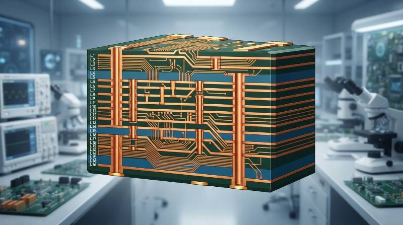
Standard Definition (IPC-2226 Type III): A printed circuit board characterized by plated microvias on both outer surfaces, containing at least two build-up layers over a core, utilizing buried vias within the core substrate, and employing through-vias connecting the outer or inner layers.Engineers deploying advanced processing units demand high-yield microvia transitions. Leveraging high-precision PCB fabrication services guarantees that dimensional changes across repeated lamination passes stay within strict multi-layer registration limits (<25 µm).
Material Selection, Dielectric Balancing, and Warpage Control
Fabricating a 3+N+3 stackup without severe thermomechanical defects requires materials engineered for high thermal stability. Because the laminate experiences four lamination cycles plus secondary solder assembly reflows, using laminates with a glass transition temperature (Tg) ≥ 170°C and a decomposition temperature (Td) ≥ 340°C is non-negotiable. The Z-axis coefficient of thermal expansion (CTE) must remain below 3.0% (from 50°C to 260°C) to prevent microvia barrel separation and barrel cracking in buried core vias. Standard low-Tg FR-4 exhibits excessive Z-axis expansion during multiple lamination cycles, generating interfacial shear stresses exceeding 80 MPa at the microvia-to-target-pad junction.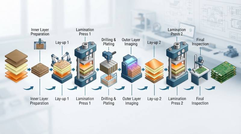
- Symmetrical Copper Distribution: Maintain copper area densities within a 5% differential between opposing mirrored layers (e.g., L1 vs. L10, L2 vs. L9) to avoid unbalanced tensile strain.
- Equalized Prepreg Stackups: Balance dielectric glass styles and resin volumes across the central core axis to eliminate asymmetric shrinking forces.
- Low-Dk / Low-Df Substrates: For high-frequency interfaces, utilize low-loss polyphenylene oxide (PPO) or modified epoxy blends to maintain controlled impedance tolerances within ±5%.
Microvia Reliability Engineering: Stacked vs. Staggered Microvias
In a 3+N+3 stackup, interconnecting L1 to L4 can be realized via stacked microvias (vias placed directly on top of each other) or staggered microvias (vias laterally offset by at least one diameter). While stacked microvias maximize routing density under dense Ball Grid Arrays (BGAs), they introduce significant thermomechanical stress concentration at the copper-to-copper interfaces.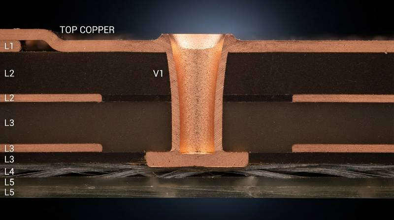
Engineering Insight: Staggered microvias exhibit higher thermomechanical fatigue life by dissipating Z-axis strain laterally into the dielectric. When layout density forces stacked microvias, IPC-6012 Class 3 rules mandate a minimum copper wrap plating thickness of 5 µm (0.0002 in) around the knee of the via to mitigate corner cracking.Laser drilling parameters determine the geometry of microvia sidewalls. Target an aspect ratio (dielectric thickness to drill diameter) of ≤ 0.8:1, with an optimal ratio of 0.65:1. An aspect ratio above 1.0:1 impedes uniform electrolyte circulation inside the hole during electrolytic copper plating, causing center-fill voids and compromised mechanical integrity.
Via-in-Pad Plated Over (VIPPO) and IPC-4761 Via Protection
Ultra-fine pitch components (e.g., 0.35mm and 0.4mm pitch BGAs) leave no room for conventional "dog-bone" fanout routing. Designers must place vias directly within the SMT landing pads. Implementing Via-in-Pad Plated Over (VIPPO / POFV) according to IPC-4761 Type VII requires void-free copper electroplating followed by mechanical planarization. Incomplete planarization or under-filled microvias leave dimples deeper than 10 µm. During reflow, surface dimples entrap air and flux, producing solder voids exceeding 25% of the total pad area. Upfront execution of a comprehensive PCB DFM review verifies that microvia fill plating, cap thickness (≥ 12 µm), and planarization meet strict Class 3 planarity standards (< 5 µm surface topography variance).Hybrid Laminate Configurations in High-Speed 3+N+3 Stackups
To balance cost with RF and high-speed digital performance (such as 112G PAM4 and PCIe Gen 6), hybrid build-ups are common in 3+N+3 architectures. High-speed, low-loss materials (e.g., Panasonic Megtron 6/7, Rogers RO4000 series, or Isola Tachyon 100G) form the outer microvia build-up layers (L1-L3 and L(N)-L(N-2)), while cost-effective standard mid/high-Tg FR-4 serves as the internal mechanical core. Heterogeneous lamination introduces CTE mismatches across core and prepreg interfaces. The X-Y CTE differential between hybrid materials must not exceed 3 ppm/°C. Failure to match curing profiles and resin flow properties can cause delamination during the 3rd and 4th lamination cycles.Comprehensive DFM & Fabrication Tolerance Specification Matrix
Fabrication tolerances for 3+N+3 HDI stackups demand rigorous process control across Laser Direct Imaging (LDI), UV/CO2 laser drilling, and acid copper electroplating baths. The following parameters represent standard vs. advanced manufacturing limits for reliable production.| Parameter | Standard Production | Advanced Capability | Critical Failure Mechanism |
|---|---|---|---|
| Laser Microvia Diameter | 100 µm (4.0 mil) | 65 – 75 µm (2.5 – 3.0 mil) | Poor plating aspect ratio, electrolyte starvation |
| Microvia Aspect Ratio | 0.75 : 1 | 0.65 : 1 | Incomplete copper fill, plating voiding |
| Microvia Capture Pad (Top) | Via + 150 µm (6.0 mil) | Via + 100 µm (4.0 mil) | Annular ring breakout, drill breakout shorts |
| Inner Target Pad Diameter | Via + 175 µm (7.0 mil) | Via + 125 µm (5.0 mil) | Missed target pad due to lamination shift |
| Line Width / Space (L/S) | 65 / 65 µm (2.5 / 2.5 mil) | 40 / 40 µm (1.6 / 1.6 mil) | Etch undercutting, open/short circuits |
| Microvia Copper Wrap Thickness | > 5 µm (IPC Class 2) | > 8 µm (IPC Class 3) | Corner knee cracking under thermal fatigue |
| Dielectric Thickness (Per Layer) | 60 – 80 µm | 40 – 50 µm | Dielectric breakdown voltage degradation |
| VIPPO Surface Dimple Depth | < 10 µm | < 5 µm | Solder paste voiding in fine-pitch BGA joints |
Architecture Comparison: 2+N+2 vs. 3+N+3 vs. Any-Layer HDI (ELIC)
Selecting the appropriate HDI architecture requires balancing escape routing constraints against overall fabrication complexity and yield dynamics. Moving from 2+N+2 to 3+N+3 introduces an additional sequential lamination cycle, tightening mechanical tolerances across all production stages. Every Layer Interconnect (ELIC) or Any-Layer HDI eliminates the mechanical core entirely, utilizing laser microvias through every individual layer. While Any-Layer offers maximum routing freedom, it demands significantly more plating passes and carries a cost premium of 40% to 70% over a 3+N+3 configuration. A 3+N+3 stackup provides an optimal compromise: it enables breakout for 0.4mm pitch ICs while retaining a rigid internal core that reduces overall warpage.- 2+N+2 Buildup: 3 total lamination cycles. Best suited for 0.5mm pitch BGAs, moderate-density wearables, and standard automotive compute boards.
- 3+N+3 Buildup: 4 total lamination cycles. Optimal for 0.4mm and 0.35mm pitch BGAs, multi-SoC boards, AI edge devices, and 5G networking modules.
- Any-Layer HDI (ELIC): N sequential lamination passes. Reserved for ultra-compact devices (smartphones, optical transceivers) where component placement is dense on both surfaces.
The Visianda EMS Multi-Lamination Thermal Balance & Microvia Qualification Protocol
To eliminate microvia failure modes and control multi-cycle registration shifts, Visianda EMS applies a specialized quality framework for all 3+N+3 HDI builds: The Octa-Thermal & Microvia Integrity Framework. This proprietary 5-step process manages yield risk across both fabrication and SMT reflow stages.- Advanced Stackup CTE & Rheology Modeling: Prior to tooling, Finite Element Analysis (FEA) simulates resin cure dynamics and thermomechanical stress distributions across all four press cycles to confirm symmetrical shear dissipation.
- UV/CO2 Laser Trepanning Optimization: Combining UV lasers (for copper ablation) with CO2 lasers (for dielectric removal) prevents undercut glass fibers and creates clean 80° tapered microvia sidewalls.
- Void-Free Superfilling Electroplating: High-purity acid copper plating baths with active leveler, suppressor, and brightener additives deliver bottom-up filling, ensuring <1% voiding rates within microvias.
- Interconnect Stress Testing (IST) Screening: Test coupons embedded in the production panel undergo 6x reflow simulations at 260°C, followed by DC thermal cycles from 25°C to 150°C, monitoring microvia resistance changes to within ±3%.
- Dynamic SMT Warpage Shadow Moire Profiling: 100% verification of bare boards under simulated thermal reflow conditions confirms board warpage remains strictly under 0.5%.
Turnkey SMT Assembly & Fine-Pitch BGA Escape Routing
Assembling 3+N+3 HDI boards with components featuring pitches ≤ 0.4mm requires tight coordination between bare-board fabrication tolerances and Surface Mount Technology (SMT) processes. Standard dog-bone routing cannot escape high-pin-count BGAs at this density without causing trace shorting or violating minimum line/space rules.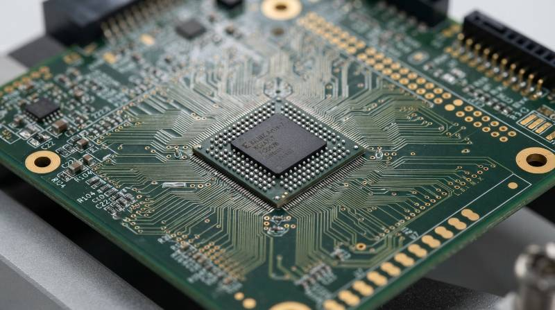
- 3D Solder Paste Inspection (3D SPI): Measures 100% of deposited paste volumes, flags bridge risks, and detects offsets across fine-pitch arrays.
- 3D Automated X-ray Inspection (3D AXI / Computed Tomography): Inspects hidden solder balls under BGAs, confirming voiding stays below 15% and validating that VIPPO pads do not cause internal micro-voids.
- Multi-Zone Reflow with Nitrogen Purge: 10-to-12 zone convection reflow ovens maintain peak temperatures between 240°C and 245°C under an N2 atmosphere (<500 ppm O2) to optimize wetting without exceeding the material's thermal threshold.
Frequently Asked Questions (FAQ) About HDI 3+N+3 Stackup Fabrication
What is the typical fabrication cycle time for a 3+N+3 HDI PCB?
Standard quick-turn prototyping for 3+N+3 HDI typically spans 10 to 14 business days due to the 4 sequential lamination, desmear, and microvia electroplating passes. Production volume runs average 3 to 4 weeks depending on hybrid material availability and specific surface finish requirements (e.g., ENIG vs. ENEPIG).Why are staggered microvias generally preferred over stacked microvias?
Staggered microvias laterally distribute thermal expansion stresses across the dielectric matrix during solder reflow. Stacked microvias create continuous vertical copper columns that concentrate Z-axis strain, increasing the risk of interface separation, target pad pull-off, or knee cracking under IPC Class 3 thermal stress tests.How is the microvia aspect ratio calculated in HDI stackups?
Aspect ratio is calculated as the thickness of the target dielectric layer divided by the top diameter of the laser-drilled microvia hole ($AR = \frac{\text{Dielectric Thickness}}{\text{Drill Diameter}}$). For robust copper plating superfilling, this ratio should not exceed 0.8:1, with 0.65:1 considered ideal for manufacturing yields.What surface finish is best suited for 0.4mm pitch BGAs on 3+N+3 boards?
Electroless Nickel Electroless Palladium Immersion Gold (ENEPIG) or Electroless Nickel Immersion Gold (ENIG) are preferred. ENEPIG eliminates the risk of "black pad" corrosion defects and provides superior planarity for wire bonding and fine-pitch BGA soldering.Ready to Optimize Your 3+N+3 HDI Stackup for High-Yield Assembly?
Partner with Visianda EMS for end-to-end high-density interconnect fabrication, advanced DFM validation, and turnkey SMT assembly.
Request a Technical DFM Review