
Core Thermal Physics: LED Junction Temperature (Tj) and Dissipation Limits
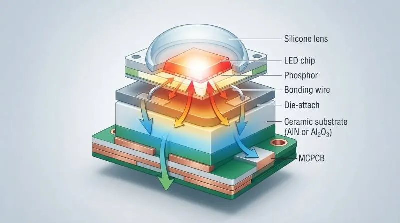
Evaluating an MCPCB assembly manufacturer for high-power LED thermal management requires verifying their ability to maintain junction temperatures ($T_j$) below critical thermal ceilings through low-void vacuum soldering and high-conductivity substrate fabrication. Standard FR4 boards fail when dissipating heat fluxes above 10 W/cm², causing thermal runaway, correlated color temperature (CCT) shifting, and rapid luminous flux loss. High-power solid-state lighting arrays (operating from 3W to over 50W per package) convert roughly 60% to 80% of input electrical power directly into waste heat. Without an optimized thermal conduit, heat concentrates at the sub-millimeter die layer.Thermal Impedance Equation: $T_j = T_a + (P_d \times R_{th,j-a})$ Where $T_j$ is Junction Temperature, $T_a$ is Ambient Temperature, $P_d$ is Power Dissipation (Watts), and $R_{th,j-a}$ is Total Thermal Resistance from junction to ambient (°C/W).For industrial floodlights, automotive headlamps, and horticultural luminaires, maintaining an LED die below its rated limit (typically 85°C to 105°C for extended L90 life) requires cutting every millikelvin of thermal resistance along the stackup path. An inadequate MCPCB assembly manufacturer will inadvertently introduce microstructural defects that choke thermal dissipation, as outlined in testing guidelines from JEDEC Standards (JESD51 series).
Substrate Engineering: Evaluating Dielectric and Base Material Performance
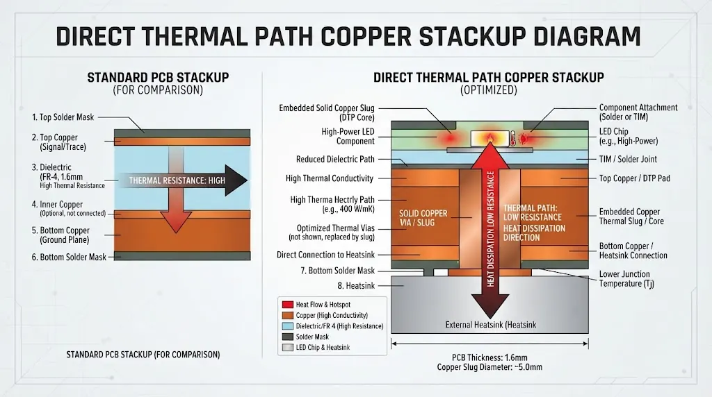
Insulated Metal Substrates (IMS) and Direct Thermal Path (DTP) boards replace standard epoxy glass with aluminum or copper carrier plates. The primary thermal barrier inside an MCPCB is the thermally conductive dielectric layer. Standard dielectric prepregs offer a meager 1.0 to 1.5 W/m·K. Advanced ceramic-filled polymers deliver between 3.0 and 8.0 W/m·K with dielectric breakdown ratings exceeding 3 kV to 6 kV AC. When evaluating rapid prototype PCBA capabilities, verify whether the manufacturer fabricates both standard dielectric layers and Direct Thermal Path copper substrates.| Substrate Architecture | Base Material | Dielectric Thermal Cond. (W/m·K) | Dielectric Breakdown (kV/mil) | Best Application |
|---|---|---|---|---|
| Standard FR4 | Glass/Epoxy | 0.25 – 0.35 | >1.0 | Low-power signal, <1W LEDs |
| Aluminum IMS (5052) | 5052 Aluminum | 1.5 – 3.0 | ≥3.0 | General commercial lighting |
| High-Performance IMS | 6061-T6 Aluminum | 4.0 – 8.0 | ≥4.5 | High-bay, stadium lighting |
| Direct Thermal Path (DTP) | C1100 Pure Copper | 385 – 400 (Direct) | N/A (Pedestal Direct) | Automotive LED headlights, COB arrays |
Precision SMT Assembly Challenges for High-Thermal-Mass Metal Backings
Surface mount assembly on metal core substrates behaves radically differently than standard PCB manufacturing. A thick aluminum or copper core acts as a massive heatsink inside the reflow oven, pulling thermal energy away from component pads. Without precision thermal profiling, this high thermal inertia leads to severe manufacturing defects: cold solder joints, uneven wetting, and tombstoning of adjacent passive components. Tier-1 precision SMT assembly services address this by using 10-to-12-zone reflow ovens equipped with bottom-side infrared or convection boosting.Engineering Insight: At Visianda EMS, our engineers maintain a maximum temperature delta ($\Delta T$) of ≤5°C across the entire MCPCB panel during reflow. We accomplish this by embedding multi-channel thermocouples directly into the metal core substrate during profile calibration.Furthermore, coefficient of thermal expansion (CTE) mismatches between the base metal (Aluminum CTE: ~23 ppm/K, Copper: ~17 ppm/K) and the LED ceramic packages (AlN/Al2O3 CTE: ~5-7 ppm/K) cause dynamic warping during heating. Mechanical bow and twist must be controlled within ≤0.5% in compliance with IPC-6012 and IPC-A-600 standards to prevent solder joint shear and delamination under heatsink mounting torque.
Solder Joint Integrity: Vacuum Reflow and 3D AXI Voiding Benchmarks
For high-power LED emitters (such as Cree XLamp, Lumileds LUXEON, or Osram OSLON), the solder joint directly underneath the thermal slug serves as the primary heat transmission pathway. Solder voids contain trapped air or outgassed flux vapors with a thermal conductivity of roughly 0.026 W/m·K, acting as thermal insulators. When voiding under the thermal pad exceeds 25%, LED operating junction temperatures spike by 15°C to 25°C. This drastic rise causes rapid lumen depreciation, localized hotspots, and premature bonding-wire fracture.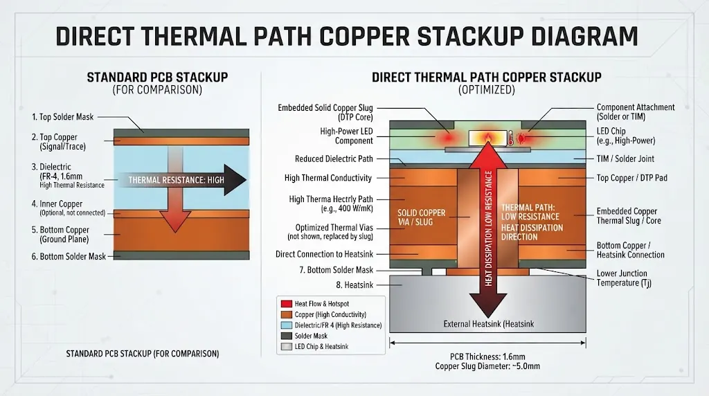
The Visianda EMS Thermal-SMT Assurance Protocol
To eliminate high-power LED field failures, Visianda EMS executes a proprietary 5-phase validation methodology designed specifically for metal core assemblies.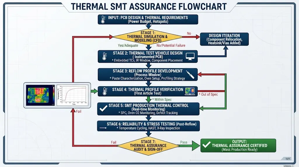
- Substrate Hi-Pot & Dielectric Verification: Every bare metal core batch undergoes 100% high-potential voltage proofing (≥3.0 kV AC / 50 Hz for 60s) to guarantee isolation resistance (>100 MΩ) and identify micro-fractures in the dielectric.
- Dynamic DFM Profiling: We design custom solder paste aperture geometries with cross-hatch/window-pane stencil openings to facilitate gas outgassing channels prior to vacuum exposure.
- Vacuum Depressurization SMT: Reflow execution inside a multi-zone vacuum chamber eliminates micro-voids beneath center LED thermal pads to meet strict ≤10% void thresholds.
- 3D AOI with Reflective White Mask Algorithms: High-reflectivity white solder masks frequently cause optical distortion on conventional AOI. We utilize multi-angle color spectrum 3D AOI to verify solder fillet height without false errors.
- Post-Assembly TIM Coplanarity Inspection: Automated laser profilometry scans the rear metal surface to confirm total flatness within 0.05 mm, ensuring gap-free coupling with external chassis and thermal interface materials (TIM).
Manufacturer Audit & Quality Checklist: Selecting the Right Turnkey EMS Partner
Procurement and engineering teams should use this technical audit checklist when assessing Tier-1 EMS suppliers for heavy-duty metal core manufacturing.| Audit Domain | Technical Requirement / Specification | Verification Standard |
|---|---|---|
| Quality Certification | Active IATF 16949 & ISO 9001 certifications | Third-party registrar audit trail |
| Reflow Equipment | Vacuum-assisted inline reflow with ≥10 heating zones | Real-time vacuum trace logs (<20 mbar) |
| Voiding Benchmarks | <10% total voiding on LED thermal slugs, <5% single void | 100% 3D AXI sample testing per lot |
| Solder Mask Integrity | Non-yellowing white solder mask (≥85% initial reflectivity) | Spectrophotometer color stability testing |
| Component Sourcing | Franchised supply channels with LED binning control (Flux, CCT, Vf) | CoC & Traceability documentation |
| Panel Depaneling | Stress-free CNC milling or V-scoring with zero delamination | Strain gauge edge analysis (<500 με) |
Frequently Asked Questions: MCPCB Assembly for High-Power LEDs
Why is copper base MCPCB superior to aluminum for ultra-high power LEDs?
Copper features a bulk thermal conductivity of ~390-400 W/m·K, compared to ~130-200 W/m·K for standard 5052/6061 aluminum alloys. Furthermore, copper accommodates Direct Thermal Path (DTP) configurations where the LED thermal pad solders directly to the metal core, bypassing the polymer dielectric layer entirely.How does solder mask discoloration affect high-power LED performance?
Standard liquid photoimageable (LPI) solder masks yellow or degrade when exposed to continuous high temperatures and short-wavelength light. This discoloration reduces luminaire optical efficiency by 3% to 8% over time. High-temperature reflective white solder masks retain >85% reflectivity under harsh conditions.What causes metal core PCBs to bow or twist during SMT reflow?
Bow and twist stem from differences in the coefficient of thermal expansion (CTE) between the thick metal base plate and the upper copper/dielectric layers. Uneven heating rates across the oven further amplify mechanical stress. Proper fixture support and balanced thermal profiling keep warpage below 0.5%.What is the acceptable solder void percentage under LED thermal pads?
While IPC-A-610 permits up to 25% or 30% voiding on general bottom-termination components, high-power LED thermal pads require voiding levels below 10% to 15% (with no single void exceeding 5%) to avoid localized hot spots and LED junction degradation.Ready to Optimize Your High-Power LED Thermal Architecture?
Partner with Visianda EMS for precision MCPCB fabrication, low-void vacuum reflow SMT assembly, and end-to-end IATF 16949 quality compliance.
Request an Engineering DFM Review