
Turnkey vs. Consignment: Selecting the Optimal Assembly Model
Low volume turnkey PCB fabrication and assembly delivers complete hardware production—from bare-board fabrication and component procurement to Surface Mount Technology SMT assembly and functional testing—under a single manufacturing partner. By consolidating bare PCB fabrication, component sourcing, SMT, and testing under one roof, engineering teams eliminate vendor fragmentation, cut prototype lead times by up to 40%, and isolate design issues before committing to mass production.
| Operational Parameter | Full Turnkey | Partial Turnkey | Consigned / Kitted |
|---|---|---|---|
| Component Sourcing | 100% EMS partner sourced via Tier-1 distribution | Client supplies custom ICs; EMS sources passives/standard parts | 100% Client kitted and shipped |
| Attrition & Scrap Liability | Managed & absorbed by EMS provider | Split liability based on component assignment | Client must supply +5% to +10% overage |
| Procurement Overhead | Zero client administration required | Moderate internal administration | High (manual PO generation, kitting, tracking) |
| Lead Time Predictability | Synchronized PCB fabrication and parts delivery | Variable depending on client shipment speed | High risk of line stoppages due to missing components |
| DFM / DFA Integration | Pre-procurement engineering scrub | Partial review prior to receiving stock | Post-delivery discovery of design mismatches |
The KVisianda EMS 5-Stage Zero-Defect NPI Protocol
To eliminate costly revisions and bridge the gap between initial prototyping and scalable mass production, Visianda EMS applies a structured manufacturing methodology. The 5-Stage Zero-Defect NPI Protocol guarantees product integrity across low-volume manufacturing runs.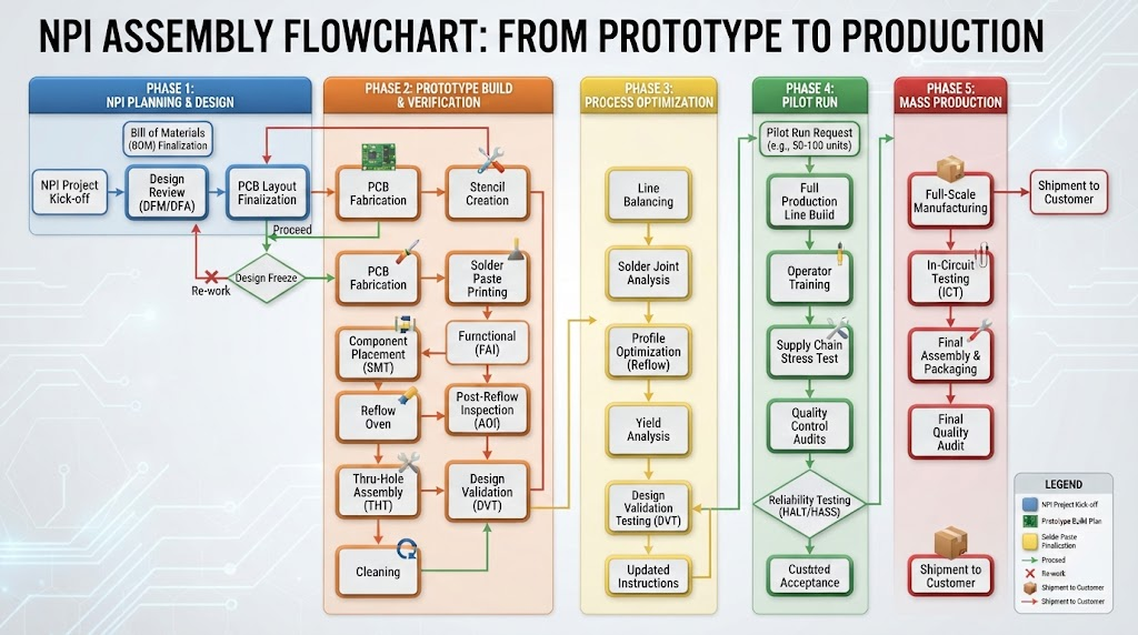
Stage 1: Pre-Flight DFM/DFA & BOM Scrubbing
Before releasing copper to the etching line, engineering conducts a multi-vector rule check on Gerber RS-274X files and ODB++ datasets. This includes validating annular rings, trace clearances, via aspect ratios, and footprint compatibility against manufacturer pinouts.Stage 2: Tier-1 Sourcing & Incoming Material Verification
Every active and passive component is sourced exclusively from franchised distributors. Incoming shipments undergo incoming lot traceability verification, moisture level checks (MSD), and packaging inspection in accordance with IPC/JEDEC J-STD-033 guidelines.Stage 3: Thermal Profiling & High-Precision Surface Mount Placement
Laser stencils with electro-polished nanocoatings ensure consistent solder paste release down to 0.3mm aperture pitches. Advanced Pick and Place Automation systems accurately place components down to 01005 passives and 0.35mm pitch fine-pitch BGAs. Reflow profiles are optimized using 10-zone nitrogen reflow ovens to prevent thermal shock.Stage 4: Automated Optical & 3D X-Ray Inspection
Every small-batch board undergoes 100% Automated Optical Inspection AOI to verify component alignment, polarity, and fillet geometry. Bottom-terminated components (BTCs, QFNs, and BGAs) are evaluated via 3D Automated X-ray Inspection (AXI) to ensure solder voiding stays below 15% across all thermal pads.Stage 5: Firmware Injection, In-Circuit Testing, and Validation
Boards undergo In-Circuit Testing ICT and flying probe analysis to verify impedance matching, power rail isolation, and passive values. Custom test jigs execute automated functional test routines and flash customer firmware to validate the circuit prior to sign-off.Engineering Insight: "Our empirical NPI data indicates that 82% of small-batch assembly errors originate from footprint mismatches and library pad misalignments, not machine placement drift. Front-loading automated DFM and BOM scrubbing prevents 99% of assembly-line stoppages."
Technical Capabilities & Manufacturing Tolerance Matrix
Small-batch turnkey manufacturing must not compromise on precision. High-density, high-speed, and mission-critical designs require stringent manufacturing controls compliant with IPC-A-610 Class 2 and Class 3 Standards.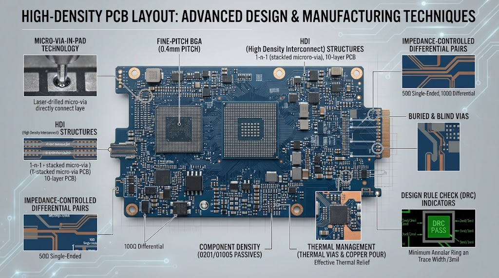
| Technical Parameter | Standard Capability | Advanced / High-Density Capability |
|---|---|---|
| Layer Count | 1 – 16 Layers | Up to 32 Layers (Rigid, Flex, Rigid-Flex) |
| Min. Trace Width / Spacing | 3.5 mil / 3.5 mil (0.089mm) | 2.5 mil / 2.5 mil (0.0635mm) |
| Smallest SMD Package | 0201 imperial | 01005 imperial / 03015 metric |
| Fine-Pitch BGA Placement | 0.50mm pitch | 0.35mm micro-BGA pitch |
| PCB Substrate Materials | FR-4 (Tg 150°C - 170°C) | Rogers, Megtron 6, Polyimide, Isola 370HR |
| Surface Finishes | HASL (Lead-Free), ENIG | ENEPIG, Immersion Silver, Hard Gold |
| Manufacturing Standards | IPC-A-610 Class 2 | IPC-A-610 Class 3, J-STD-001 Space/Medical |
Pre-Production DFM and DFA Engineering Checklist
A successful low-volume run depends on resolving physical layout defects before generating SMT tooling. Ensure your CAD packages satisfy these critical Design for Manufacturing DFM and Design for Assembly DFA rules:- Thermal Relief Symmetry: Verify balanced copper connections on surface mount pads. Unequal thermal mass between dual terminals (e.g., 0402/0201 passives) causes premature solder paste liquefaction on one side, leading to tombstoning.
- Solder Mask Dams: Maintain a minimum 3 mil (0.075mm) solder mask dam between adjacent fine-pitch QFP or IC pads to prevent solder bridging during reflow.
- Fiducial Placement: Include at least three global fiducials on panel margins and two local diagonal fiducials for fine-pitch ICs (pitch ≤ 0.5mm). Ensure a 1.0mm clearance zone free of copper and solder mask around all fiducial targets.
- Component Clearances: Maintain at least 0.5mm clearance between SMT passives and tall electrolytic capacitors or connectors to prevent optical shadowing during AOI and pick-and-place nozzle collisions.
- Via-in-Pad Protection: Fill and cap (IPC-4761 Type VII) or plug any vias located directly within thermal or SMT landing pads to avoid solder wicking away from critical component joints.
Supply Chain Integrity: Anti-Counterfeit and Traceability Protocols
Component integrity is critical for modern electronic hardware. Counterfeit components and unauthorized brokers introduce catastrophic functional anomalies that escape standard basic testing. Within the Visianda EMS Manufacturing Ecosystem, electronic component sourcing is conducted exclusively through direct API integration with authorized Tier-1 distributors—including Digi-Key, Mouser Electronics, Arrow Electronics, and Future Electronics. Every incoming lot is cataloged with manufacturer part numbers (MPNs), date codes, and Certificates of Conformance (COC).Traceability Standard: Component management complies strictly with ISO 9001:2015 traceability audits. Active and passive devices are tracked from receiving, through reel barcode assignment, to the exact board serial number produced on the line.When encountering component obsolescence or extended factory lead times, our component engineering team recommends pin-compatible and functional alternatives. We conduct footprint validation and circuit simulation before implementing any design updates.
Rigorous Quality Assurance: AOI, X-Ray (AXI), and Functional Testing
Small-batch assembly requires advanced verification across every unit. Unlike high-volume mass production, which relies on statistical sample testing, low-volume turnkey manufacturing requires 100% board-level inspection.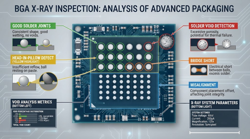
- 3D Automated Optical Inspection (AOI): Evaluates solder fillet curvature, component presence/absence, pin misalignment, and solder bridge anomalies across all SMD joints.
- 3D Automated X-Ray Inspection (AXI): Delivers non-destructive inspection of concealed solder joints beneath Ball Grid Arrays (BGAs), Quad Flat No-leads (QFNs), and Land Grid Arrays (LGAs). We verify uniform ball collapse and keep void area below 15%.
- Through-Hole Assembly THT Verification: Wave and selective soldering joints are checked against IPC-A-610 Class 3 specifications for vertical barrel fill (>75%) and uniform 360° top/bottom fillet development.
- Flying Probe & Functional Test (FCT): Validates circuit nets for shorts and opens without expensive custom bed-of-nails fixtures. Custom test jigs power on boards and execute real-world operational testing.
Turnkey Value-Added Services: Beyond the Bare Board
Modern hardware teams need comprehensive manufacturing partners who can handle everything beyond basic SMT placement. Scaling an NPI prototype to market requires system-level execution. Visianda EMS provides turnkey backend integration, enabling engineering teams to receive fully assembled, market-ready products:- Firmware Flashing & Pre-Programming: In-system programming (ISP) and off-line socket programming for microcontrollers, FPGAs, EEPROMs, and flash memory.
- Selective Conformal Coating: Automated spray application of acrylic, silicone, or polyurethane coatings to protect against moisture, salt spray, and particulate contamination.
- Custom Wire & Cable Harnesses: Precision crimp-and-poke, overmolded connectors, and ribbon cable assemblies manufactured to exact specifications.
- Mechanical Integration & Box-Build: Complete final assembly, integrating custom extruded enclosures, injection-molded plastics, fasteners, displays, and internal cabling.
Engineering Case Study: Resolving Thermal Tombstoning on a 0201 IoT Pilot Run
A prominent medical IoT device company engaged Visianda EMS to manufacture a pilot batch of 150 dense, 8-layer HDI sensor boards. Initial low-volume prototype builds at another manufacturing facility suffered a high defect rate: 18.5% of 0201 decoupling capacitors experienced severe tombstoning (vertical chip lifting), causing production delays.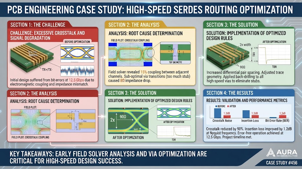
Root Cause Analysis
Visianda EMS production engineers conducted thermal cross-section imaging and Gerber audit analyses, identifying two primary root causes:- Unbalanced Pad Heat Sinking: One pad of the 0201 capacitor was tied directly to a continuous inner ground plane without thermal relief, while the opposing pad connected to a narrow 4 mil signal trace. The ground plane sank heat rapidly, creating a 12°C delta during solder reflow that caused uneven wetting tension.
- Excessive Solder Paste Deposition: The customer-specified 5 mil laser-cut stencil deposited excessive paste volume relative to the micro-pads, pulling the passives upright during surface tension development.
Engineering Resolution & Results
Our team implemented a three-part corrective action plan:- Redesigned the stencil layout using a 3.5 mil electro-formed foil with home-plate aperture geometry, reducing paste volume by 22%.
- Added thermal relief neck-downs to the high-density copper plane pads in the manufacturing tooling layer.
- Tuned our 10-zone nitrogen reflow oven profile, extending the soak zone by 18 seconds to ensure uniform board temperatures before liquidus.
Lead Time Breakdown & Sourcing-to-Delivery Timeline
Speed to market is essential during NPI. Turnkey manufacturing streamlines timelines by synchronizing bare-board fabrication with electronic component procurement.| Timeline Phase | Key Engineering & Operational Milestones | Deliverables / Output |
|---|---|---|
| Day 1 – Day 2 | Pre-flight DFM review, BOM validation, and distributor PO release. | DFM approval sign-off; Sourcing pipeline active. |
| Day 3 – Day 6 | Parallel bare PCB fabrication and Tier-1 component shipping. | Bare boards drilled, plated, and electrically tested (E-tested). |
| Day 7 – Day 8 | SMT laser stencil generation, SMT high-speed placement, and nitrogen reflow. | Fully assembled PCBA surface mount topside/bottomside. |
| Day 9 – Day 10 | THT wave soldering, 3D AOI/AXI inspection, ICT/functional testing, and vacuum packaging. | Final QA inspection report, CoC certificate, and secure dispatch. |
Frequently Asked Questions (FAQ)
What is the minimum order quantity (MOQ) for low-volume turnkey PCBA?
Visianda EMS has no minimum order quantity. We support pilot runs ranging from 1 to 5 prototype units up to pilot production runs of several thousand boards.What engineering files are required for an accurate turnkey quote?
To generate an accurate quote and run a pre-flight DFM scrub, submit your complete Gerber RS-274X or ODB++ files, Bill of Materials (BOM) in Excel format with complete MPNs and designators, Centroid/Pick-and-Place (X-Y coordinate) file, and fabrication assembly drawings.How do you manage moisture-sensitive devices (MSD) during assembly?
All moisture-sensitive devices are cataloged and handled strictly per IPC/JEDEC J-STD-033 standards. Components exceeding floor-life exposure are baked in temperature-controlled dry cabinets prior to SMT reflow to prevent package delamination and micro-cracking.How does Visianda EMS protect client intellectual property (IP)?
We implement strict Non-Disclosure Agreements (NDAs), encrypted CAD handling, isolated server networks, and restricted production-floor access to ensure proprietary designs and firmware remain secure.Accelerate Your Hardware Development Cycle
Transition your designs smoothly from CAD layout to fully tested, production-grade hardware. Contact Visianda EMS for a pre-flight DFM engineering audit and competitive turnkey manufacturing quote.
Request a Turnkey Quote