
What Defines Full Turnkey PCB Assembly?
A full turnkey PCB assembly Shenzhen manufacturer manages the complete electronics production lifecycle, consolidating bare circuit board fabrication, active and passive component procurement, surface-mount assembly, and end-of-line functional validation under a single purchase order. This model eliminates multi-vendor coordination bottlenecks, transferring supply chain risk and manufacturing liability entirely to the electronic manufacturing services (EMS) provider. In modern contract manufacturing, procurement strategies fall across a spectrum of supplier engagement. Choosing the right structure dictates your engineering overhead, inventory holding liability, and production velocity.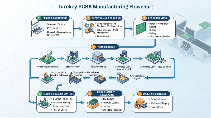
| Dimension | Full Turnkey | Partial Turnkey | Consigned (Kitted) |
|---|---|---|---|
| Component Sourcing | 100% EMS Managed | Client supplies key ICs; EMS sources passives | 100% Client Supplied |
| PCB Fabrication | EMS Handled | EMS or Client | Client Supplied |
| Procurement Lead Time | Optimized via local Shenzhen hub | Moderate (Split tracking) | High (Client manages logistics) |
| Quality Liability | Single-source EMS accountability | Shared (Component vs. Assembly) | Split between vendor and fabricator |
The Visianda 6-Stage Traceable Turnkey Protocol
To eliminate systematic assembly escapes, our production facility deploys The Visianda 6-Stage Traceable Turnkey Protocol. This systematic workflow maintains rigorous process governance across engineering reviews, supply chain execution, and physical assembly.The 6 Production Gates
- Gate 1: Multi-Vector DFM/DFA Verification — Automated netlist cross-checks, component footprint clearance validation, and solder mask expansion reviews.
- Gate 2: Authorized Supply Line Procurement — Direct purchasing via franchised distributors, pairing parts with Certificate of Conformance (CoC) tracking.
- Gate 3: Incoming Material Quality Control (IQC) — X-ray fluorescence (XRF) alloy checks, moisture barrier bag (MBB) verification, and solderability tests per IPC/J-STD-002.
- Gate 4: High-Precision SMT & Closed-Loop SPI — Solder paste deposition monitoring, high-speed pick-and-place, and multi-zone reflow with nitrogen inerting.
- Gate 5: Automated Defect Screening — Dual-track inline 3D AOI alongside 3D Automated X-ray Inspection (AXI) for non-visible interconnects.
- Gate 6: End-of-Line Functional Testing & Serialization — Full-load ICT, custom functional verification (FCT), barcode serialization, and anti-static ESD packaging.
Advanced SMT & DIP Manufacturing Infrastructure in Shenzhen
Shenzhen's manufacturing advantage relies on dense equipment clusters and mature component support ecosystems. Tier-1 facilities feature high-speed SMT lines capable of sub-millimeter component placement with tight spatial tolerances.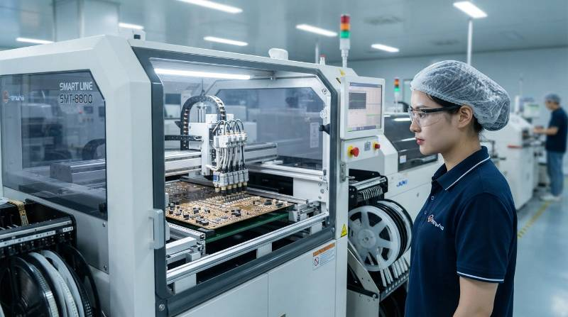
Surface-Mount Capabilities & Technical Tolerances
- Placement Precision: High-speed Yamaha and Panasonic modular mounters achieving ±0.025 mm (±25 μm) at 3-sigma repeatability.
- Micro-Component Handling: Standard volume support down to 01005 (0402 metric) passives and 0.3 mm pitch fine-pitch ball grid arrays (BGA) and quad-flat no-leads (QFN) packages.
- Reflow Profiling: 10-zone to 12-zone forced-air convection reflow ovens with independent top/bottom closed-loop temperature control and real-time oxygen monitoring (<500 ppm O2).
Component Sourcing Integrity & Anti-Counterfeit Verification
Component integrity represents the largest operational risk in turnkey electronics manufacturing. Open-market broker sourcing creates exposure to remarked dies, refurbished pulls, and sub-standard silicon."Counterfeit electronic components are non-conforming parts deliberately misrepresented in identity, performance, or traceability, presenting catastrophic failure risks in mission-critical applications."
Multi-Stage Incoming Screening Protocol
To secure our supply chain, Visianda EMS sources direct from factory-authorized channels including DigiKey, Mouser Electronics, Arrow Electronics, and Element14, supplemented by direct semiconductor factory lines.- XRF Material Screening: Verifies lead-free RoHS compliance and authenticates terminal metallization alloys against supplier datasheets.
- Chemical Resistance / Acetone Wipe Testing: Identifies blacktopping and re-marked packaging using aggressive solvent wiping per SAE AS5553 standards.
- Die Decapsulation & Microscopic Analysis: Exposes silicon dies under high-magnification optical inspection to verify manufacturer logos, mask markings, and internal wire bonds.
- Moisture Sensitivity Management: Automated dry cabinets tracking J-STD-033 floor life for MSL 3, 4, 5, and 6 components with integrated thermal desiccant baking.
Rigorous Quality Control: 3D SPI, AXI, and IPC Standards
Over 70% of SMT assembly defects originate during solder paste printing. Preventing these escapes requires closed-loop inspection checkpoints along the entire production line.
Inspection Gate Specifications
- Inline 3D Solder Paste Inspection (SPI): Real-time volumetric measurement monitoring paste height, volume, area, and bridging. Automatically adjusts the screen printer alignment using closed-loop feedback.
- Inline 3D Automated Optical Inspection (AOI): Multi-angle telecentric lens arrays measuring component coplanarity, solder fillet height, tombstoning, reversed polarity, and text recognition via optical character verification (OCV).
- High-Resolution 3D Automated X-ray Inspection (AXI): Calculates BGA and QFN voiding ratios under oblique angles. Our standard threshold maintains voiding below 15% across all joints—well inside the 25% IPC-A-610 Class 3 limit.
Comprehensive In-Circuit, Functional (FCT), and Burn-In Testing
Optical checks confirm physical placement, but electrical testing validates operational performance under real-world operating conditions.Downstream Electrical Test Methodologies
- In-Circuit Testing (ICT): Dedicated bed-of-nails test fixtures verifying component values, passive tolerances, open traces, and short circuits across specific test points.
- Flying Probe Testing: Fixtureless electrical testing optimal for rapid turnaround prototypes, low-volume NPI batches, and dense board layouts.
- Functional Circuit Testing (FCT): Custom test jigs simulating true end-device operating environments, driving power rails, measuring RF signals, and verifying communications buses (CAN, I2C, SPI, UART).
- Automated Firmware Flashing: Secure, isolated firmware programming paired with unique MAC address assignment and digital cryptographic signature verification.
- Thermal Chamber Burn-In: Dynamic thermal cycling (typically -40°C to +85°C or +125°C) under electrical load to eliminate infant mortality failures on mission-critical assemblies.
Navigating High-Mix, Low-to-Medium Volume (HMLV) Production
Shenzhen's manufacturing ecosystem accommodates agile production runs alongside mass-market throughput. This structure is built for high-mix, low-to-medium volume (HMLV) projects that require rapid iteration without excessive overhead. Flexible feeder carts, intelligent part replenishment scanners, and offline feeder preparation allow engineering teams to cut tooling changeovers to under 15 minutes. This supports small-batch builds without large minimum order quantities (MOQs).Factory Audit & Supplier Vetting Checklist for Global Procurement
When auditing a turnkey PCBA partner in Shenzhen, technical buyers must look beyond headline equipment lists. Evaluate process discipline, factory floor controls, and certifications directly.| Audit Category | Key Technical Verification Criteria | Standard Requirement |
|---|---|---|
| Quality Management Systems | Active ISO 9001, ISO 13485 (Medical), IATF 16949 (Automotive) certificates with accredited registrar verification. | ISO 9001:2015 / ISO 13485 |
| ESD Control Protocols | Conductive epoxy flooring, continuous wrist-strap monitoring, ionizers at pick-and-place stations, surface resistance <1.0×10⁹ ohms. | ANSI/ESD S20.20-2021 |
| Moisture & Chemical Storage | Nitrogen-purged dry boxes (<5% RH), automated MSL logging, calibrated desiccant baking ovens. | IPC/JEDEC J-STD-033D |
| Process Traceability | Laser-etched 2D DataMatrix serialization linking board ID to component reel lot numbers, reflow profiles, and operator IDs. | Full Level 3 Traceability |
| Intellectual Property Security | Enforceable Non-Disclosure Agreements (NDAs), isolated internal testing networks, air-gapped programming stations. | Strict NNN Agreements |
Box-Build Integration and Final Electro-Mechanical Packaging
Turnkey manufacturing extends past bare board assembly. High-reliability applications often require complete electro-mechanical box-build assembly to package electronics for immediate commercial deployment.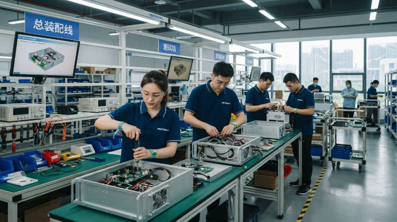
End-to-End Box-Build Services
- Conformal Coating: Automated selective spray coating (acrylic, polyurethane, silicone) per IPC-CC-830 standards to protect assemblies against moisture, dust, and harsh environments.
- Potting & Encapsulation: Dual-component epoxy or polyurethane potting for high-vibration, sub-sea, or high-voltage applications.
- Precision Enclosure Integration: Clean-room assembly of custom CNC aluminum, sheet metal, and injection-molded plastics with accurate torque-controlled fastening.
- Wire Harness & Cable Loom Fabrication: Automated wire stripping, crimping, heat-shrink tagging, and continuity testing.
Frequently Asked Questions About Turnkey PCB Assembly in Shenzhen
What are standard lead times for turnkey PCB assembly?
Prototype runs typically ship in 3 to 7 business days following DFM approval and component receipt. Full production orders generally require 3 to 5 weeks, depending on component lead times and bare board fabrication schedules.How do you handle hard-to-find components or parts with long lead times?
We flag supply risks during our initial BOM scrub and suggest drop-in form-fit-function (FFF) alternatives. Our engineering team never substitutes any component without explicit written authorization and revised engineering approval.Which IPC manufacturing standard is followed?
All production lines assemble boards to IPC-A-610 Class 2 standards by default. For medical, aerospace, and critical industrial platforms, we manufacture and inspect to IPC-A-610 Class 3 and J-STD-001 requirements upon request.How is intellectual property protected during manufacturing?
We protect design assets with bilingual non-disclosure agreements, air-gapped programming fixtures, and strict role-based data access policies across our internal engineering networks.Accelerate Your Hardware Production with Visianda EMS
Upload your Gerber files and Bill of Materials to receive a comprehensive DFM engineering review, verified component pricing, and a detailed manufacturing quote within 24 hours.
Request Your Turnkey Quote