Space Environment Challenges: Designing PCBAs for Low Earth Orbit Survivability
LEO satellite turnkey PCB assembly requires ultra-high-reliability manufacturing practices engineered to withstand severe thermal swings (-65°C to +125°C), high-vacuum outgassing, atomic oxygen erosion, and intense launch vibration. Achieving full mission capability demands strict adherence to IPC Class 3 and space-grade screening standards across all fabrication, assembly, and testing phases. Deploying avionics hardware to Low Earth Orbit (altitudes between 160 km and 2,000 km) introduces environmental stressors unseen in terrestrial or aviation electronics. In the vacuum of space, convective cooling does not exist. Heat dissipation relies entirely on direct thermal conduction through the PCB stackup and outward radiative dissipation. Solder joints undergo extreme thermomechanical stress during the 14 to 16 orbital cycles experienced every 24 hours. Without meticulous strain-relief design and void-free soldering, standard assemblies suffer micro-cracking and early fatigue failure.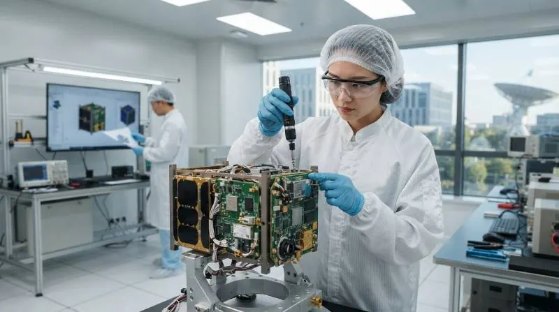
Radiation Mitigation: Total Ionizing Dose (TID) and Single-Event Effects (SEE)
LEO satellites pass continuously through the South Atlantic Anomaly (SAA) and auroral zones, exposing onboard avionics to trapped protons and high-energy cosmic rays. Total Ionizing Dose (TID) accumulates in semiconductor silicon over time, causing threshold voltage shifts, increased leakage current, and eventual functional failure. Single-Event Effects (SEE)—such as Single-Event Upsets (SEU), Single-Event Functional Interrupts (SEFI), and catastrophic Single-Event Latchup (SEL)—pose instantaneous risks to digital processing nodes. For small satellite constellations, mission architectures balance radiation-hardened components with radiation-tolerant Commercial-Off-The-Shelf (COTS) devices supported by hardware-level watchdog circuits and current-limiting power switches.Total Ionizing Dose (TID): The cumulative ionizing radiation absorbed by an electronic component over its operational lifetime in orbit, measured in kilorads (krad(Si)).For standard 3 to 5-year LEO missions, electronic sub-assemblies typically require radiation tolerance between 10 krad(Si) and 30 krad(Si). In contrast, critical payload and attitude determination systems often demand up to 50 krad(Si) or higher.
Material Selection & Outgassing Control Under ASTM E595
In high vacuum, volatile organic compounds within standard FR-4 laminates, solder pastes, adhesives, and conformal coatings evaporate rapidly. This outgassed material condenses on sensitive optics, solar arrays, and high-voltage sensors, causing payload blinding or electrical shorting. All flight hardware must comply with the ASTM E595 test standard, maintaining a Total Mass Loss (TML) of <1.00% and a Collected Volatile Condensable Material (CVCM) rating of <0.10%.| Laminate Material | Tg (°C) | CTE Z-Axis (ppm/°C) | TML (%) | CVCM (%) | Primary Application |
|---|---|---|---|---|---|
| Polyimide (e.g., Ventec VT-901) | >250 | 30 – 40 | 0.35 | 0.01 | High-Layer Flight Computers, Power Distribution |
| High-Tg FR-4 (e.g., Isola 370HR) | 180 | 45 | 0.65 | 0.02 | Standard CubeSat Bus Avionics |
| PTFE / Hydrocarbon (e.g., Rogers 4350B) | >280 | 32 | 0.08 | 0.00 | S-Band / X-Band RF Transceivers |
| High-Speed Low-Loss (e.g., Megtron 6) | 185 | 40 | 0.42 | 0.01 | High-Speed Payload Data Recorders |
Turnkey SMT & Through-Hole Manufacturing for Space Avionics
Hardware teams building space electronics require end-to-end turnkey PCB assembly solutions executed under strict Class 3 cleanroom protocols. Soldering standards for space hardware do not permit commercial concessions. All assembly processes must comply directly with IPC J-STD-001 Class 3 Space Addendum, IPC-A-610 Class 3, and NASA-STD-8739. Flight boards undergo automated optical inspection (AOI) alongside rigorous manual visual verification by certified IPC trainers under 10x to 40x stereomicroscopy.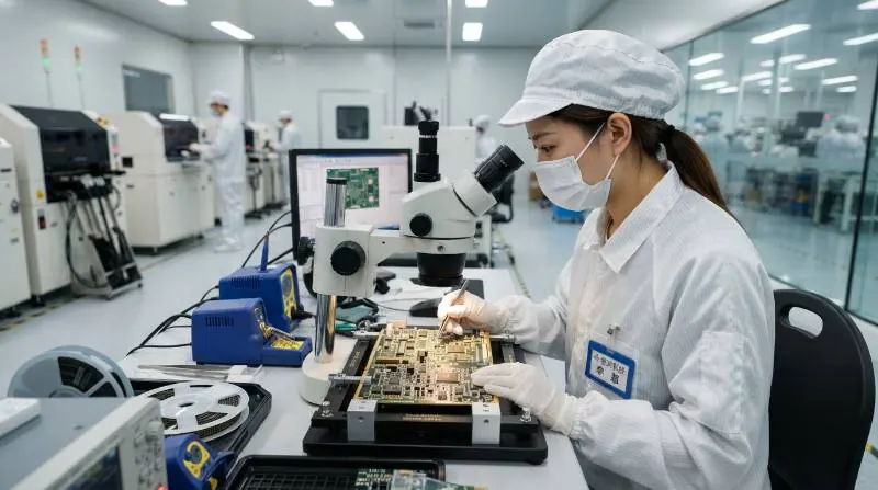
Eliminating Solder Voiding: Vacuum Reflow Techniques for High-Density BGAs & QFNs
Under terrestrial conditions, a 15% to 25% solder void rate in large bottom-terminated components (BTCs) is often tolerable. In orbit, trapped gas pockets inside solder joints act as thermal barriers because vacuum prevents convective heat equalization. This trapped heat causes localized hotspots, thermal runaway, and premature mechanical fatigue under thermal cycling. Visianda EMS utilizes Vacuum Vapor Phase Reflow (VPR) systems to actively pull entrapped flux vapors from the liquidus solder bath.
The Visianda EMS SpaceFlight™ Turnkey PCBA Protocol
To eliminate mission failure risks across modern satellite constellation builds, we have developed a structured, 5-phase manufacturing framework known as The SpaceFlight™ Turnkey PCBA Protocol.- Phase 1: Space-Grade DFM/DFA Architectural Review: Comprehensive analysis of copper balance, via-in-pad capping (IPC-4761 Type VII), thermal pad venting, and stress-relief copper filleting.
- Phase 2: Authenticated OCM Component Acquisition: Sourcing strictly through Original Component Manufacturers (OCMs) or franchised distributors with lot-date traceability and anti-counterfeit screening.
- Phase 3: Ultra-Low-Void Vacuum SMT & Manual Soldering: Assembly executed in ISO 7 (Class 10,000) cleanroom environments with closed-loop vacuum vapor phase reflow profiles.
- Phase 4: Multi-Axis Metrology & Non-Destructive Inspection: 3D SPI, 3D AXI (void quantification), and high-resolution AOI compliant with IPC J-STD-001 Space Addendum.
- Phase 5: Environmental Screening & Conformal Encapsulation: Precision selective coating, vacuum bakeout, and thermal shock/TVAC validation before release.
"In space avionics, assembly anomalies that appear harmless on the ground cause catastrophic subsystem loss in orbit. Standard commercial reflow profiles leave unvented flux gases that degrade thermal pathways. Enforcing vacuum vapor phase reflow below 5% voiding is essential for orbital payload survival." — Director of Quality Assurance, Aerospace Systems DivisionDuring a recent 24-satellite constellation production run at Visianda EMS, our facility delivered 192 critical avionics modules over six months with a 0% field failure rate through 18 months of orbital operation.
COTS Upscreening vs. Rad-Hard BOM Optimization for NewSpace Constellations
Pure radiation-hardened (rad-hard) components feature extended lead times (often 40 to 60+ weeks) and unit costs that challenge commercial NewSpace budgets. Consequently, hardware engineering teams increasingly use upscreened automotive (AEC-Q100/Q200) or industrial COTS components for non-critical and redundant subsystems. Upscreening bridges this gap through rigorous post-procurement lot testing, including burn-in screening, thermal shock cycling, and electrical parameter drift testing across temperature boundaries (-55°C to +125°C).| Evaluation Parameter | Standard COTS | Upscreened Industrial / Auto COTS | Class S Rad-Hard (MIL-PRF-38535) |
|---|---|---|---|
| Unit Cost Multiplier | 1x (Baseline) | 3x – 6x (Testing overhead) | 25x – 100x+ |
| Procurement Lead Time | 2 – 8 Weeks | 8 – 16 Weeks (Including LAT) | 36 – 60+ Weeks |
| Radiation Assurance | None (Unverified) | Lot Acceptance Testing (TID/SEE) | Guaranteed (100 krad to 1 Mrad) |
| Traceability | Standard Commercial | Full Single-Lot Date Code (SLDC) | Full Wafer-Level Traceability |
| Ideal Mission Scope | Short-life Tech Demos (<6 mo) | LEO SmallSats / Constellations (2-5 yr) | Deep Space, GEO, Defense Assets |
Supply Chain Integrity, OCM Traceability, and Anti-Counterfeit Protocols
Counterfeit components pose serious risks to space hardware. A cloned or re-marked IC can function under ambient bench testing but fail instantly in a vacuum when exposed to thermal extremes. We source 100% of our active and passive components through authorized franchise distributors and direct OCM channels under AS6081 and AS9100D supply chain governance. Every component lot is registered with complete Certificates of Conformance (CoC), Single-Lot Date Codes (SLDC), and full incoming inspection documentation (including decapsulation, die marking verification, and XRF material analysis).Mission-Critical Screening: Conformal Coating, Vibration, and TVAC Testing
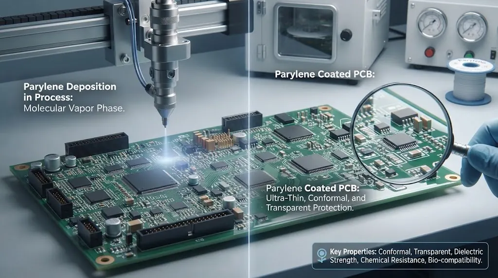
Following SMT assembly, circuit boards require robust physical protection against pure tin whisker growth, mechanical debris, and orbital plasma arcs. Tin whiskers grow spontaneously from lead-free solder finishes and can short adjacent fine-pitch IC pins in microgravity. We apply vapor-deposited Parylene C or Parylene N coatings to form a uniform, pinhole-free barrier over complex component geometries. Parylene provides exceptional dielectric strength, negligible outgassing, and total isolation from atomic oxygen erosion.