
Any-Layer HDI PCB & Laser-Drilled Microvia Architecture: Technical Foundations
Evaluating an any-layer HDI PCB microvia laser drilling manufacturer requires auditing laser-drilling registration tolerances (≤ ±12.5µm), copper superfilling chemistries, and post-lamination thermal endurance. Selecting the right fabrication partner ensures microvias maintain structural continuity across all dielectric layers without target pad separation during lead-free assembly. Standard High-Density Interconnect (HDI) boards rely on sequential build-up (SBU) schemes like 1+N+1 or 2+N+2 with a mechanically drilled core. In contrast, Every Layer Interconnect (ELIC) or Any-Layer HDI eliminates mechanical core drills entirely. Every layer pair connects via laser-ablated, electroplated solid copper microvias, allowing unrestricted routing freedom for high-pin-count silicon.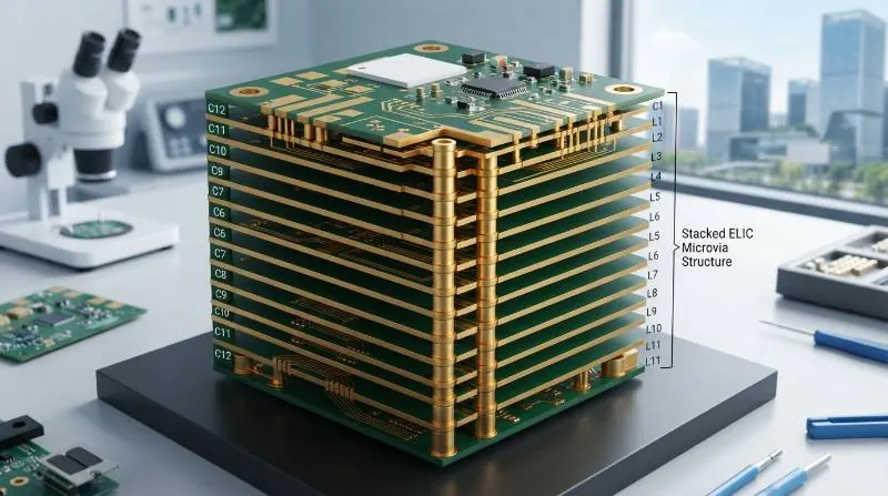
IPC-2226 Definition: An Any-Layer HDI architecture consists of structures where blind and buried microvias are populated across all conductive layers, terminated with solid copper filling to enable arbitrary z-axis interlayer routing.Maintaining high fabrication yields requires adhering to strict geometric ratios. Microvias must maintain an aspect ratio (depth-to-diameter) of ≤ 0.8:1 to 1:1. Once the dielectric thickness exceeds the hole diameter, electroplating chemistry cannot reliably circulate to replenish copper ions at the base, creating latent voiding risks.
Laser Drilling Mechanics: UV vs. CO2 Systems for Sub-75µm Microvia Integrity
Precision microvia formation relies on two primary laser optical engines: Ultraviolet (UV) solid-state lasers (typically 355nm) and pulsed Carbon Dioxide (CO2) lasers (9.4µm to 10.6µm). Each technology handles base copper foils and advanced resin-glass matrices differently. UV lasers operate via photolytic cold ablation, breaking molecular bonds directly without thermal disruption. This makes UV ideal for cutting outer copper foil windows and drilling sub-50µm microvias in Ajinomoto Build-up Film (ABF) and high-speed PTFE laminates. CO2 lasers utilize photothermal ablation, vaporizing organic resin matrices and reinforced glass bundles at extreme speeds.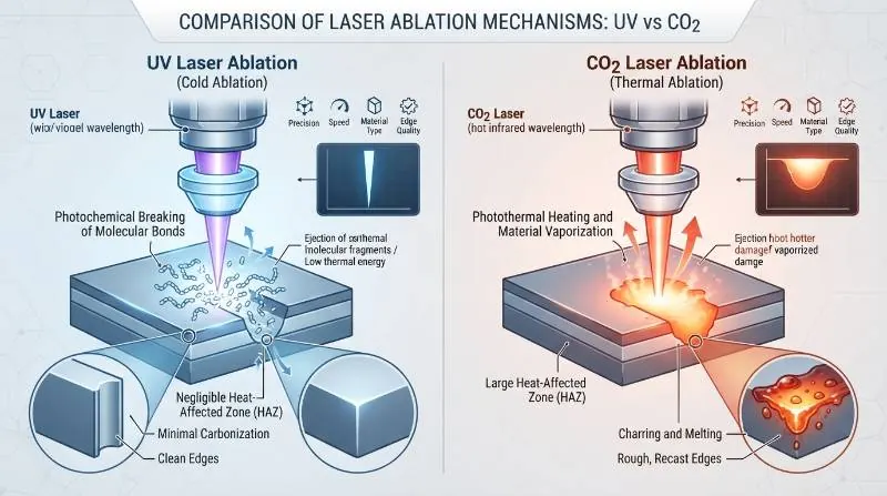
| Parameter | UV Laser (355 nm) | CO2 Laser (9.4 / 10.6 µm) | Dual-Head Hybrid |
|---|---|---|---|
| Ablation Mechanism | Photolytic (Cold Bond Cleavage) | Photothermal (Vaporization) | Sequential Photolytic / Photothermal |
| Minimum Achievable Via Diameter | 25 µm | 65 µm | 40 µm |
| Taper Angle Deviation | < 8° (Nearly vertical) | 12° to 18° (Pronounced trapezoid) | < 10° |
| Target Capture Pad Registration | ± 10 µm (LDI-guided) | ± 15 µm | ± 12.5 µm |
| Glass Fiber Weave Compatibility | Cuts glass cleanly without fiber protrusion | Deflects on heavy E-glass bundles | Optimal for spread glass (106/1080) |
Desmear and Copper Plating: Preventing Microvia Knee and Target Pad Separation
Laser drilling leaves resin smear and carbonized debris across the copper target pad. If this residue is not fully eliminated before metallization, the stacked microvia stack will separate under thermal stress. Traditional chemical sodium permanganate desmear lacks the surface tension mechanics to penetrate blind microvias below 75µm. High-reliability manufacturing lines require RF Plasma Desmear ($CF_4 / O_2$ or $Ar / O_2$ gas mixtures) to chemically volatilize resin debris inside narrow microvia barrels. Following desmear, the board enters electrolytic plating baths optimized for superconformal copper bottom-up filling. Plating baths use a balanced three-part organic additive system:- Suppressors (Carbowax/PEG): High-molecular-weight polymers that adsorb at the microvia entrance (knee) to inhibit local copper deposition.
- Accelerators (SPS/MPS): Low-molecular-weight sulfur compounds that concentrate at the microvia bottom to accelerate deposition rates.
- Levelers (JGB/Diazine Dyes): Positively charged polymers preventing nodular growth and planarizing the top surface.
Stacked vs. Staggered Microvias: Structural Reliability and Thermal Shock Performance
Any-Layer designs often force an architectural choice: stacked microvias or staggered microvias. Stacked microvias maximize routing density directly under fine-pitch BGA packages, but they concentrate z-axis thermal expansion strain directly through the metallic column.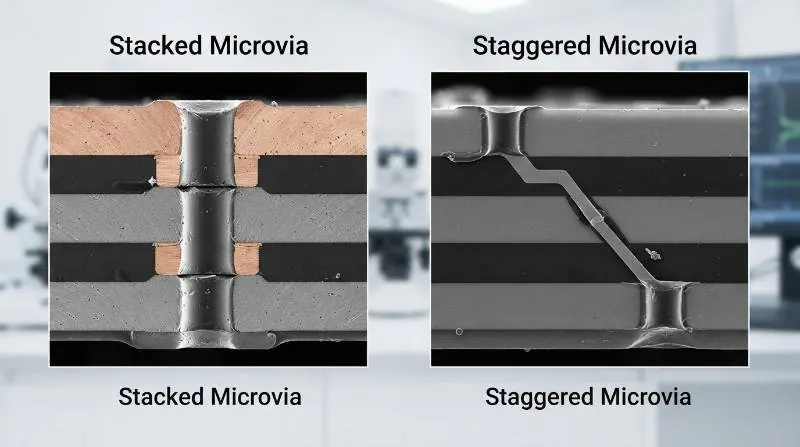
| Metric | Stacked Microvias (Type VII) | Staggered Microvias |
|---|---|---|
| Silicon Escape Routing Density | Maximum (100% Fan-in/out freedom) | Moderate (-30% channel blockage) |
| IST 260°C Thermal Cycles to Failure | 800 to 1,200 cycles | > 2,500 cycles |
| Primary Failure Mechanism | Target pad micro-separation / barrel shear | Internal trace knee fatigue |
| Plating Flatness Requirement | Strict dimple ≤ 5 µm | Moderate dimple ≤ 15 µm |
Downstream SMT PCBA Integration for Ultra-Fine Pitch 0.3mm/0.4mm Micro-BGAs
Bare-board Any-Layer fabrication must align closely with surface mount technology (SMT) constraints. Modern System-on-Chip (SoC) and Baseband processors feature 0.35mm and 0.30mm pitch array patterns that require Via-in-Pad Plated Over (VIPPO / POFV) architectures. VIPPO interfaces present two common failure points during assembly: pad surface depression (dimple) and pad protrusion (bump). An un-planarized dimple (>10µm) traps flux and air during solder paste printing, causing voiding in Bottom-Terminated Components (BTCs). Protrusions cause solder bridging between adjacent BGA balls.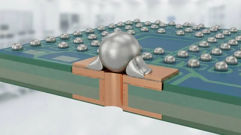
The Visianda Precision-Via Integration Protocol (KPIP)
To eliminate microvia interconnect failure modes, Visianda EMS developed a proprietary validation methodology: the Visianda Precision-Via Integration Protocol (KPIP). This framework connects raw material DFM checks directly to 3D X-ray metrology on active assembly lines.
- Phase 1: DFM Stackup & Dielectric Matrix Verification — Stackup modeling balances resin content against copper weights to eliminate laminate starvation and keep microvia aspect ratios under 0.9:1.
- Phase 2: Dynamic Dual-Beam Laser Drilling & RF Plasma Etching — Closed-loop optical fiducial mapping adjusts for substrate distortion on every panel, followed by RF plasma desmear to guarantee target pad cleanliness.
- Phase 3: Superconformal Chemical Copper Fill Control — Continuous cyclic voltammetric stripping (CVS) monitors additive bath concentrations to ensure planar copper deposits with dimples ≤ 5µm.
- Phase 4: Multi-Axis 3D AXI & Metallurgical Cross-Sectioning — High-resolution 3D Automated X-ray Inspection (AXI) confirms that solder joints on top of microvias remain free of micro-voids (<10% void volume).
Industry Applications: High-Reliability Demands in Medical, Automotive, and Aerospace
Any-Layer HDI technology is critical for next-generation hardware across complex, high-reliability sectors:- Medical Diagnostics & Implants: Wearable ultrasounds, continuous glucose monitors (CGMs), and surgical robotics demand sub-0.35mm pitch packaging within ultra-dense form factors. Visianda EMS supports these systems through certified medical electronics manufacturing compliant with ISO 13485 standards.
- Automotive ADAS & Radar Modules: 77GHz millimeter-wave radar and autonomous driving computing platforms require low-loss substrates and robust microvias that survive under-hood thermal shock. Our facilities deliver automotive-grade quality via automotive electronics PCBA processes under IATF 16949 oversight.
- Aerospace & Edge Compute: Avionics and satellite flight systems utilize stacked ELIC microvias capable of passing 288°C solder float thermal shock cycles.
Quality Assurance, Microsectioning, and Factory Audit Criteria
Procurement teams must audit a manufacturer’s physical cleanroom controls and metallurgical analysis lab before signing production contracts. Inspecting basic factory certificates is not enough to verify Any-Layer HDI capability.| Audit Area | Mandatory Inspection Metric | Class 3 Acceptance Baseline |
|---|---|---|
| Cleanroom Environmental Controls | Airborne particulate count in laser drilling & lamination bays | ISO Class 6 (Class 1,000) for imaging; ISO Class 7 (Class 10,000) for laser drilling |
| Microsectioning Metallography | Cross-section microvia inspection per production lot coupon | Zero interfacial separation; copper thickness in barrel ≥ 18 µm |
| Thermal Stress Resistance | IPC-TM-650 2.6.8 thermal solder float testing | Float at 288°C ± 5°C for 10 seconds (minimum 3 cycles without delamination) |
| High-Speed Signal Integrity | Time-Domain Reflectometry (TDR) trace coupon checks | Impedance tolerance ≤ ± 5% across single-ended and diff pairs |
| Lot Traceability Execution | Manufacturing Execution System (MES) scanning | Full 2D matrix panel-level and component-level serialized tracking |
Frequently Asked Questions About Any-Layer HDI PCB Laser Drilling Manufacturing
Why is RF plasma desmear critical for Any-Layer HDI microvias?
Chemical permanganate etch solutions cannot reliably penetrate microvias smaller than 75µm due to surface tension limits. RF plasma etching uses excited gas ions to vaporize drill smear and ensure pristine metallic bonding at the target capture pad.What causes microvia target pad separation during assembly?
Separation is typically driven by z-axis CTE mismatch between the dielectric resin and the copper barrel during 260°C lead-free reflow, exacerbated by residual smear or poor copper bath additive balance.How does VIPPO flatness affect 0.3mm pitch BGA assembly?
If the electroplated copper fill leaves a dimple > 5µm, solder paste wicks down into the recess, starving the joint and leaving structural voids. Surface bumps > 5µm create planarity mismatches that can lead to solder bridges.Engineer Your Any-Layer HDI Assembly with Visianda EMS
From sub-75µm laser drilling and Class 3 solid copper microvia filling to turnkey 0.3mm BGA surface mount assembly, Visianda EMS delivers zero-defect manufacturing for mission-critical electronics.
Request a DFM Review & Quote