
Engineering High-Performance Aluminum MCPCBs for Horticultural Lighting
Successful aluminum-backed mcpcb prototype assembly for commercial led horticultural lighting requires tight thermal dissipation matching, low-voiding solder joints under high-power emitters, and strict optical alignment. Commercial grow fixtures operate under severe continuous-current loads, where thermal mismanagement drops Photosynthetically Active Radiation (PAR) output and shifts spectral recipes. Commercial horticultural luminaires demand continuous high-flux output across strict photoperiods ranging from 12 to 20 hours daily. Under these operating conditions, junction temperatures ($T_j$) must remain tightly regulated below 85°C to prevent irreversible photon efficacy degradation ($\mu\text{mol/J}$) and spectral drift. Standard FR-4 circuit boards cannot handle the continuous heat flux generated by high-density top-bin horticultural emitters. Metal Core Printed Circuit Boards (MCPCBs) featuring a dedicated aluminum base plate provide the direct conductive path required to transfer heat away from the diode array to passive fixture extrusions.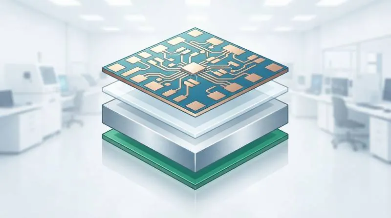
Thermal Engineering: Substrate, Dielectric, and Copper Foil Selection
The thermal stackup forms the baseline for all subsequent assembly steps. Selecting the right aluminum alloy, dielectric layer thermal conductivity, and copper weight dictates whether your horticultural fixture survives prolonged thermal cycling in damp greenhouse environments. We routinely specify between 5052 and 6061 aluminum alloys depending on fixture mechanical stress and form factor. While 5052 aluminum delivers superior workability and corrosion resistance against humid agrochemical environments, 6061-T6 provides the structural rigidity needed for long, narrow luminaire light bars exceeding 1.2 meters.| Parameter | 5052 Aluminum Alloy | 6061-T6 Aluminum Alloy |
|---|---|---|
| Thermal Conductivity (W/m·K) | 138 W/m·K | 167 W/m·K |
| Yield Strength (MPa) | 193 MPa | 276 MPa |
| Atmospheric Corrosion Resistance | Exceptional (High Mg content) | High (requires surface passivation) |
| Warpage Risk during V-Scoring | Low to Moderate | Extremely Low (High Rigidity) |
"Dielectric breakdown voltage must remain balanced against thermal impedance. Thin dielectric layers (75 µm to 100 µm) offer optimal thermal transfer, but they require precision trace routing to guarantee UL 94V-0 flammability ratings and exceed 3.0 kVAC electrical isolation."For high-current light engines wired in series-parallel configurations, 2oz (70 µm) or 3oz (105 µm) heavy copper foil is critical. Heavy copper traces reduce parasitic $I^2R$ resistive power loss, prevent localized circuit heating, and improve overall fixture photon efficacy ($\mu\text{mol/J}$). When evaluating copper weights for fast prototyping, engineers rely on our rapid prototype PCBA services to test early trace impedance models without production line delays.
Handling Mixed-Wavelength LED Arrays and Delicate Dome Optics
Horticultural fixtures rarely use a single diode package. Modern spectrum engineering combines broad-spectrum white mid-power LEDs (such as the Samsung LM301H series) with monochromatic high-power deep-red (660nm) and far-red (730nm) emitters (such as the Osram Oslon Square Hyper Red).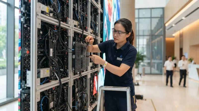
Advanced SMT Reflow Profiling on High-Mass Metal Core Substrates
Soldering components onto an aluminum-backed circuit board presents severe thermal management challenges during surface-mount processing. Because the aluminum base plate is designed to dissipate heat rapidly, it acts as a massive thermal heat sink inside the reflow oven. Standard convective reflow profiles calculated for FR-4 will trigger widespread cold solder joints, insufficient solder wetting, and severe component skewing on MCPCBs. To counteract rapid board heat absorption, our production lines utilize multi-zone reflow ovens equipped with independent high-velocity bottom-side convection heaters.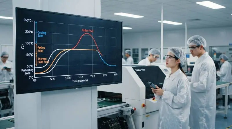
The Visianda HortiThermal™ Prototyping Protocol
To eliminate early-stage build failures and streamline time-to-market for commercial lighting OEMs, our engineering team developed a targeted, five-stage methodology: The Visianda HortiThermal™ Prototyping Protocol. This systematic approach ensures every fast-turn build transitions seamlessly into high-yield mass production.- DFM Thermal & V-Score Stress Simulation: We verify copper clearance, aluminum substrate creepage, dielectric standoff, and mechanical web thickness along V-score lines to prevent trace cracking during panel singulation.
- Radiometric & Voltage Binning Verification: Incoming optical inspection audits all LED lots to confirm forward voltage ($V_f$) grouping and photosynthetic photon efficacy matching before feeder loading.
- Substrate-Calibrated Multi-Zone Thermal Reflow: Bottom-side convective pre-heating profiles are tuned specifically to the board mass, aluminum alloy grade, and heavy-copper distribution.
- Automated 3D X-Ray Voiding & Alignment Audit: Every prototype undergoes 3D Automated X-ray Inspection (AXI) to verify that thermal pad voiding remains strictly below 15% across all mid-power and high-power footprints.
- Electrical Isolation & High-Pot Stress Screening: Boards undergo automated dielectric withstand testing up to 3.75 kVAC to confirm zero dielectric micro-fractures prior to shipping.

Environmental Resilience: Conformal Coating and Corrosion Protection in CEA
Controlled Environment Agriculture (CEA) facilities—such as vertical farms, indoor grow rooms, and commercial glass greenhouses—expose lighting assemblies to hostile operating conditions. Relative humidity often hovers between 70% and 90% RH, accompanied by airborne fertilizer compounds (ammonia, nitrates) and vaporized sulfur from pest-management burners. Sulfur vapor attacks unprotected silver plating within LED lead frames, converting reflective silver into black silver sulfide ($Ag_2S$). This reaction rapidly reduces diode photon output by up to 40% within several months of operation. Furthermore, moisture condensation on high-voltage circuit traces can trigger dendritic metal migration and dielectric flashover. To achieve IP65 to IP68 ingress protection without altering the spectral recipe, selective conformal coating is applied. Optical-grade silicone coatings provide superior ultraviolet resistance, excellent thermal stability up to 200°C, and minimal transmission loss (<1%) across the 400nm–750nm PAR spectrum. Automated selective dispensing robots apply uniform protective layers over exposed copper leads and solder fillets while masking primary silicone dome optics.Prototyping Quality Assurance: Hi-Pot, Thermal Shock, and Radiometric Testing
Prototype validation for commercial horticultural lighting requires rigorous electrical and optical testing before tooling sign-off. Horticultural luminaires frequently connect multiple MCPCB light engines in series onto constant-current drivers operating up to 400VDC or higher. Dielectric Withstand Voltage (Hi-Pot) testing validates the integrity of the thin dielectric layer separating copper circuit traces from the grounded aluminum chassis. Our testing protocols subject light bars to 1.5 kVAC to 3.75 kVAC dielectric stress testing for 60 seconds, verifying leakage currents remain safely under 2.0 mA.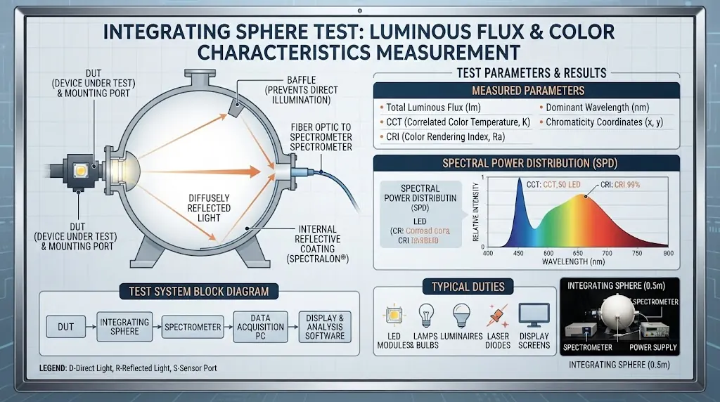
Accelerating Time-to-Market: Turnkey Prototyping with Visianda EMS
Managing multiple vendors for bare MCPCB fabrication, custom SMT stencils, diode component procurement, and final assembly introduces costly schedule slips and quality handoff risks. Turnkey manufacturing consolidates the entire development cycle under a single quality management system. By leveraging complete turnkey PCB assembly solutions, commercial lighting developers compress prototyping schedules from weeks down to 24–48 hours. Early DFM feedback identifies trace spacing bottlenecks, V-score edge margins, and solder pad footprints before fabrication begins. Visianda EMS maintains direct sourcing channels with premier horticultural LED manufacturers and dielectric substrate suppliers, guaranteeing traceable component binning and material authenticity. When you are ready to de-risk your next grow light platform, contact Visianda EMS engineering support to review your Gerber files, BOM stackup, and thermal specifications.Frequently Asked Questions (FAQs)
What is the recommended dielectric thickness for horticultural MCPCBs?
For high-performance horticultural luminaires, a dielectric layer thickness of 75 µm to 100 µm (3 to 4 mils) offers the optimal balance between high thermal conductivity (2.0 to 3.0 W/m·K) and robust dielectric breakdown isolation (typically >3.0 kVAC).Should aluminum MCPCB light bars be V-scored or tab-routed?
V-scoring is standard for linear light bars because it maximizes panel material utilization. However, you must maintain at least 0.5mm to 1.0mm trace-to-edge clearance from the V-score cut line to prevent dielectric micro-fracturing and high-voltage creepage shorts during mechanical singulation.How do you prevent excessive solder voiding on high-power LED thermal pads?
We combine optimized stencil apertures (such as cross-hatched or window-pane openings that deliver 70%–80% solder paste coverage) with vacuum reflow or multi-zone bottom-side convective pre-heating. This lets outgassing flux volatiles escape before the solder alloy solidifies.What is the standard turnaround time for aluminum MCPCB prototype builds?
Quick-turn prototype builds can be assembled and inspected in as fast as 24 to 48 hours once bare boards and component reels are verified on-site, with full turnkey fabrication and assembly typically completing within 5 to 10 business days depending on custom dielectric substrate availability.Ready to Build High-Efficacy Horticultural LED Prototypes?
Eliminate assembly risk, prevent thermal degradation, and accelerate your commercial lighting fixture launch with Visianda EMS turnkey manufacturing.
Request an Engineering DFM Review