
Understanding Express Multilayer PCBA Prototyping: Core Metrics and Baseline Pricing
Express multilayer PCB prototype assembly costs range from $800 to $3,500 for a typical 5-to-10-piece prototype run on a 24-to-72-hour turnaround. Pricing depends on raw substrate layer count, total component count (SMT and PTH placements), fine-pitch component density, and expedited engineering setups. When prototyping mission-critical electronics, production velocity directly impacts time-to-market. Securing a quick-turn prototype PCBA requires balancing rapid fabrication tooling fees against assembly changeover expenses. Express pricing separates into three primary cost centers: bare-board fab expediting, SMT stencil tooling/machine setup, and active assembly cycle time.
| Layer Stackup | Fabrication Base | SMT Tooling & Setup | Placement Cost / Board | Est. Total Range |
|---|---|---|---|---|
| 4-Layer (Standard FR-4) | $250 - $450 | $300 - $500 | $35 - $75 | $750 - $1,450 |
| 6-Layer (High-Tg FR-4) | $450 - $750 | $350 - $600 | $55 - $110 | $1,100 - $2,100 |
| 8-Layer (Controlled Impedance) | $700 - $1,200 | $400 - $700 | $70 - $140 | $1,500 - $2,800 |
| 10 to 12-Layer (Microvias/HDI) | $1,200 - $2,200 | $500 - $850 | $100 - $200 | $2,300 - $4,200+ |
Core Engineering Cost Drivers in Multilayer PCB Prototype Assembly
Every mechanical and electrical parameter in your design alters fabrication yield, pick-and-place indexing speed, and automated inspection profiles. Managing prototype expenses requires identifying which design choices trigger exponential cost increases.Layer Count Multipliers: 4-Layer vs. 8-Layer vs. 12+ Layer Stackups
Increasing layer count adds sequential lamination cycles, internal copper etching steps, and chemical oxide treatments. While a 4-layer stackup requires a single press cycle, an 8-layer HDI board with blind or buried vias requires multiple lamination and laser micro-drilling sequences.Controlled impedance tolerances under ±5% on high-speed inner layers add 15% to 25% to raw board fabrication costs due to coupon coupon verification and dielectric thickness adjustments.In our manufacturing experience, specifying standard ±10% impedance tolerances rather than tightening down to ±5% prevents yield-related rush remakes and reduces base fabrication fees.
Component Packaging Density: Fine-Pitch BGAs, QFNs, and 0201 Passives
Component density directly governs feeder assignments and machine head travel speeds during SMT assembly. Populating miniature 0201 or 01005 passives demands specialized micro-nozzles, lower pick-and-place indexing speeds, and laser-cut nano-coated stencils to achieve reliable solder paste release. Executing precision SMT assembly for ball grid arrays (BGAs) with ball pitches below 0.4 mm introduces double-sided reflow challenges and mandatory X-ray validation routines.- Laser-Cut Electroformed Stencils: Adds $250 to $450 for stepped or nano-coated foils to handle mixed-pitch footprints.
- Double-Sided SMT Reflow: Increases assembly setup charges by 60% to 80% due to dual stencil alignment and second-pass thermal profiling.
- High Feeder Counts: Boards exceeding 60 unique Line Item counts require dual-gantry pick and place machine setups, raising line setup costs.
Laminate Selection: Standard FR-4 vs. High-Tg vs. Rogers Materials
Raw substrate core materials dictate thermal survival during lead-free SAC305 assembly cycles. Lead-free reflow profiles reach peak temperatures of 245°C to 260°C, making material selection crucial for multilayer board integrity. Using standard FR-4 (Tg 130°C–140°C) on an 8-layer prototype risks z-axis barrel cracking and delamination. High-Tg FR-4 (Tg 170°C–180°C, such as Isola 370HR or Shengyi S1000-2) provides the required thermal reliability for multi-cycle assembly, adding only an 8% to 15% raw material cost delta. High-frequency hybrid stackups (e.g., Rogers 4350B paired with FR-4) increase raw core costs by 200% to 400% compared to standard FR-4. They also require custom drilling feeds and specialized plasma surface preparation during fabrication.Turnkey vs. Consigned Express Prototype Assembly: TCO and Lead-Time Risk
Engineering teams face a fundamental choice between fully consigned (kitted) assembly and complete turnkey procurement. While consigned models appear cheaper on paper, hidden logistical friction often derails express timelines. Opting for turnkey PCB assembly services consolidates bare board fabrication, active component procurement, and automated assembly under single-source accountability.| Operational Metric | Full Turnkey Model | Consigned / Kitted Model |
|---|---|---|
| Procurement Lead Time | Parallel processing during PCB fab | Sequential (Customer kitting & shipping) |
| Component Shortage Risk | Immediate authorized distributor stock matching | Line stoppage if attrition margin is missing |
| Engineering Hold Liability | EMS provider resolves DFM/BOM issues | Customer assumes delay fees during holds |
| Total Cost of Ownership (TCO) | Lower overall indirect overhead | High internal engineering hours required |

The Visianda 4-Stage Express Velocity Protocol™ for Rapid PCBA
To eliminate typical quick-turn production delays, Visianda EMS applies a proprietary manufacturing workflow. The Visianda 4-Stage Express Velocity Protocol™ compresses standard 10-day cycles down to 24 to 72 hours without skipping IPC-A-610 workmanship verifications.- Stage 1: Automated Pre-DFM & Solderability Scrub Within 2 hours of RFQ submission, Gerbers and BOMs undergo parallel automated Design for Manufacturing (DFM) and Design for Assembly (DFA) checks. We identify solder bridge risks, pad mismatch errors, and footprint anomalies before raw copper enters the chemical line.
- Stage 2: Dynamic Parallel Turnkey Component Sourcing Bare board fabrication runs concurrently with electronic component fulfillment. Direct API integration with tier-1 authorized distributors allows us to lock in and verify genuine parts before the laminated panels exit solder mask curing.
- Stage 3: High-Speed Modular SMT Setup & Intelligent Reflow Dedicated quick-turn lines use offline setup carts and intelligent feeder trolleys to achieve near-zero line changeover times. Customized thermal profiling matches the exact thermal mass of the multilayer board and its active BGA packages.
- Stage 4: In-Line Multi-Tiered Quality Verification Completed boards transition directly into automated optical inspection (AOI) and 3D automated X-ray inspection (AXI) to verify internal solder joints, followed by optional flying probe continuity tests.
Inspection, Quality Assurance, and Hidden Multipliers: 2D/3D AXI for BGAs
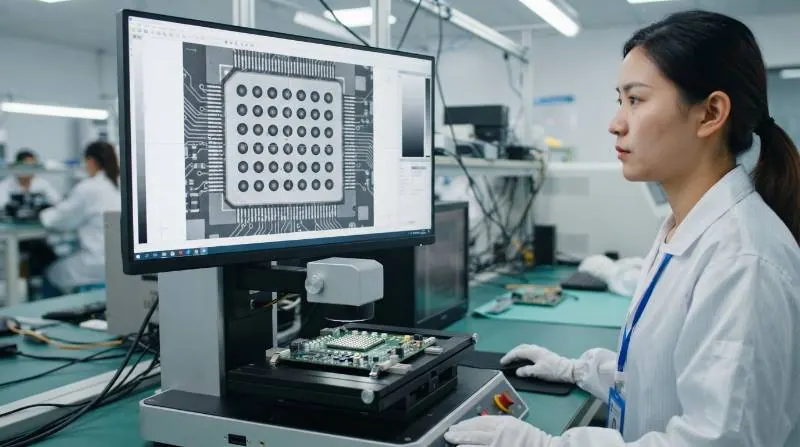
High-density multilayer designs place complex bottom-terminated components (BTCs) such as BGAs, QFNs, and LGA modules on outer layers. Visual inspection cannot confirm hidden solder integrity beneath package perimeters.Compliance with IPC-A-610 Class 2 and Class 3 workmanship standards limits acceptable BGA solder voiding to under 25% of the total ball projection area.Automated X-ray Inspection (AXI) adds $150 to $400 to an express prototype build. However, this testing cost is minimal compared to the expense of debugging board interconnect shorts on an active bench prototype.
- 2D Automated Optical Inspection (AOI): Validates component orientation, polarity, solder bridge defects, and tombstoning on passives down to 0201 sizes.
- 3D Automated X-ray Inspection (AXI): Scans through internal ground planes to detect hidden ball bridging, non-wetting opens, and excess voiding beneath BGA arrays.
- Flying Probe Testing: Electrically tests bare and assembled nets without expensive custom bed-of-nails fixtures, adding $200 to $500 per prototype run.

RFQ Submission Checklist: Avoiding Engineering Holds on Rush Prototypes
Over 60% of quick-turn production delays stem from incomplete or conflicting RFQ documentation. Submitting complete, clean manufacturing packages prevents engineering holds and locks in target shipping schedules.| Document File | Required Format | Critical Details Included |
|---|---|---|
| PCB Layout Data | ODB++, IPC-2581, or Gerber RS-274X | Drill files, IPC netlist, copper layer stackup drawing |
| Bill of Materials (BOM) | .XLSX or .CSV | Full MPN, Reference Designators, Footprint, Approved Alternate MPNs |
| Centroid (Pick & Place) | ASCII / Text / .CSV | RefDes, X/Y coordinates, Layer (Top/Bottom), Rotation angles (0-360°) |
| Fabrication Notes | PDF / ReadMe | Final thickness (e.g. 1.6mm), Copper weight (1oz/2oz), Surface finish (ENIG/HASL), Solder mask color |
| Assembly Drawing | Pin 1 indicators, polarized caps, special mechanical torque specs |