
Automotive LED Headlight PCB Fabrication & Heavy Copper SMT Assembly Overview
Automotive LED headlight PCB fabrication and heavy copper SMT assembly combine specialized thick-copper substrate manufacturing (3oz to 6oz+) with high-precision surface mount assembly to manage severe thermal densities in modern Adaptive Driving Beam (ADB) and Matrix LED headlamps. Operating under IATF 16949 and IPC Class 3 standards, this engineering approach dissipates junction temperatures exceeding 125°C while guaranteeing structural integrity under intense thermal shock and mechanical vibration. Modern automotive forward lighting has transitioned from static illumination to dynamic matrix modules containing dozens of individually addressable high-power emitters. Delivering drive currents from 1.5A to over 3.0A per channel inside sealed, space-constrained headlamp housings creates severe localized heat flux. Managing this heat requires dedicated automotive electronics manufacturing expertise. Every phase—from raw copper etching to vapor-phase vacuum soldering—must be strictly controlled to eliminate catastrophic lumen depreciation and optical shift over a vehicle's operating lifetime.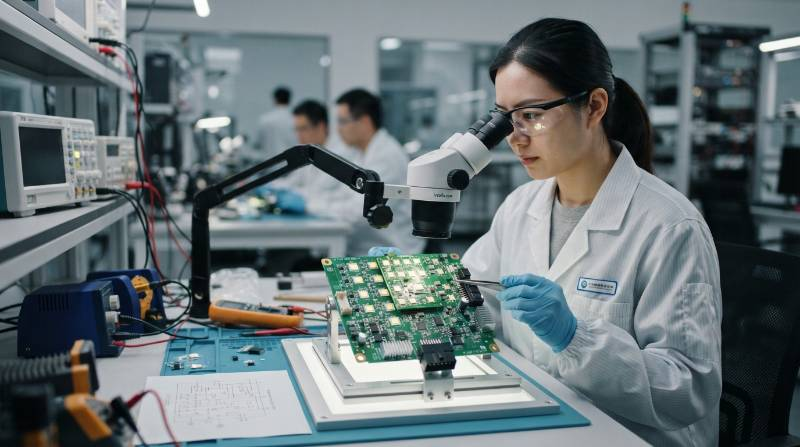
Thermal Architecture: Heavy Copper FR-4 vs. Metal Core PCB (MCPCB)
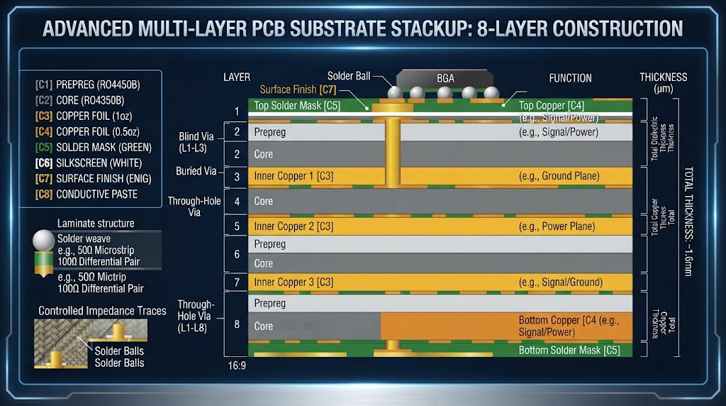
Selecting the correct substrate architecture forms the foundation of exterior lighting thermal management. Automotive hardware designers must balance thermal resistance (Rth), signal routing density, dielectric breakdown voltage, and total stackup cost.
Direct Thermal Path (DTP): A substrate design where the LED thermal pad mounts directly onto an integrated copper pedestal, bypassing the dielectric layer entirely to achieve thermal conductivity ratings above 380 W/m·K.While standard Single-Layer Aluminum MCPCBs offer an economical solution for low-complexity daytime running lights (DRLs), advanced Matrix LED and ADB modules demand multi-layer signal routing for CAN/LIN transceivers, buck drivers, and multiplexers. In these scenarios, heavy copper FR-4 with copper-filled microvias (VIPPO) or Direct Thermal Path copper-base boards become mandatory.
| Substrate Type | Thermal Conductivity (W/m·K) | Routing Layers | Breakdown Voltage (kV/mm) | CTE Mismatch vs. Ceramic LED |
|---|---|---|---|---|
| Standard FR-4 (1oz) | 0.3 - 0.5 | 1 - 32+ | > 30 | Moderate (14-17 ppm/°C) |
| Heavy Copper FR-4 (4oz + Thermal Vias) | 2.5 - 4.5 (Effective) | 2 - 16+ | > 30 | Moderate (14-17 ppm/°C) |
| Aluminum MCPCB (High-Tg Dielectric) | 3.0 - 8.0 | 1 - 2 | 3 - 5 | High (22-24 ppm/°C) |
| Direct Thermal Path (DTP) Copper Base | 380 - 400 | 1 - 4 | N/A (Direct Pad) | Low-Moderate (16-17 ppm/°C) |
Tj) by up to 18°C on 15W emitter clusters. This drop directly protects phosphor layers from accelerated thermal breakdown.
Heavy Copper PCB Design & Fabrication Engineering Nuances
Fabricating circuit boards with copper weights ranging from 3oz (105 µm) to 6oz (210 µm) introduces severe chemical and mechanical constraints that standard PCB processes cannot tolerate. Etching heavy copper conductors without proper process compensation results in pronounced trapezoidal trace geometry, known as undercut.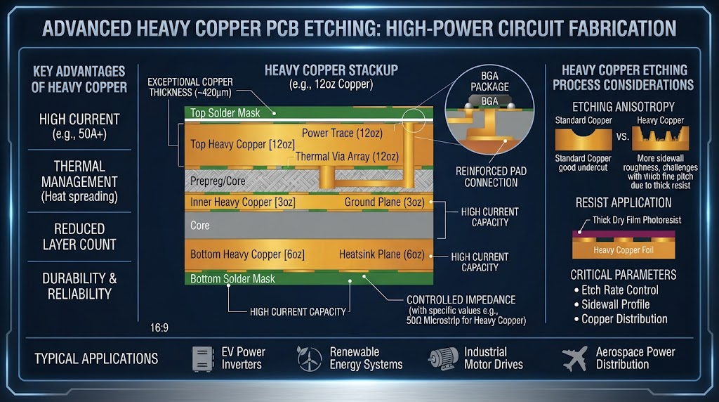
Etch Factor Ratio: Etch Factor = Total Copper Thickness (T) / Lateral Undercut Depth (U). For 4oz outer-layer copper, fabrication requires an etch compensation factor of at least 3:1 to preserve design trace widths within ±10% tolerance.Engineers must incorporate specific Design for Manufacturing (DFM) rules during trace layout:
- Conductor Spacing: Maintain minimum trace-to-trace spacing of at least 0.25 mm (10 mil) for 3oz copper and 0.40 mm (16 mil) for 6oz copper to guarantee clean etchant evacuation.
- Resin Starvation Prevention: Heavy copper inner layers require high-resin prepregs (such as 1080 or 2116 with >55% resin content) to fill deep conductor valleys and avoid delamination voids under thermal cycling.
- Thick Solder Mask Deposition: Standard curtain coating fails over 150 µm copper steps. Double-coat electrostatic spray or liquid photoimageable (LPI) screening must be used to ensure at least 25 µm edge coverage over conductor corners.
High-Power LED SMT Assembly: Tackling High Thermal Mass Sinking
Assembling high-power ceramic LED packages (such as Osram Oslon Black Flat, Lumileds LUXEON Rebel, and Cree XLamp) onto heavy copper substrates creates distinct challenges during surface mount processing. The thick copper planes act as massive heat sinks during reflow. This causes a wide thermal delta (ΔT) across the assembly, where small passive components overheat while large LED thermal pads remain below liquidus temperature.
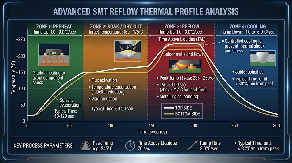
- Stepped Stencils: Step-up stencils (e.g., 100 µm base with 130 µm raised zones) deposit adequate solder paste on thick thermal lugs while preventing bridging on fine-pitch 0.5 mm driver IC pins.
- Aperture Window-Paring: Segmenting thermal slug apertures into window-pane patterns (65% to 75% area coverage) creates natural outgassing channels for flux volatiles.
- Optimized Solder Pastes: Using low-voiding, halogen-free Type 4 or Type 4.5 SAC305/SACX pastes matches high-thermal-mass reflow curves without premature flux exhaustion.
The Visianda EMS Zero-Void Heavy Copper Reflow Protocol
To eliminate reliability issues caused by excessive solder voids, Visianda EMS applies a proprietary 5-stage manufacturing protocol specifically optimized for high-power automotive exterior lighting.- Automated Optical Stencil Metrology: 3D SPI measures paste volume, height, and area across 100% of apertures to catch deposition drift before placement.
- Dual-Zone Nitrogen Inertion: Reflow zones are inerted to <100 ppm O2 levels, cutting oxidation on thick copper lands and promoting uniform wetting.
- Sub-Atmospheric Vacuum De-Gassing: Liquidus-phase vacuum chambers lower chamber pressure to <10 mbar, pulling trapped volatiles and flux out of the melt within 15 to 30 seconds.
- Inline 3D Computed Tomography (AXI): Micro-focus X-ray systems inspect 100% of LED thermal interfaces, rejecting boards exceeding a 5% total void threshold or individual voids above 2%.
- CTE-Matched Environmental Sealing: Automated conformal coating protects the board edges from sulfur corrosion, moisture ingress, and thermal-mechanical shock.
Mitigating Solder Voiding on High-Power LED Thermal Pads
Trapped gas under high-flux LEDs creates localized thermal bottlenecks. Because heat cannot transfer efficiently into the copper core, current crowding and hot spots form within the semiconductor die. Over time, these hot spots cause wavelength drift (chromaticity shift), accelerated luminous flux decay, and eventual solder fatigue cracking. By maintaining total voiding below 5% in accordance with IPC-6012 Automotive Class 3 guidelines, automotive headlights maintain consistent luminous output and color temperature across their full operating lifespan.
Quality Assurance, IATF 16949 Standards & Environmental Stress Screening
Automotive headlamps endure severe environmental conditions: ambient temperatures under the hood cycling from -40°C to +105°C, high humidity, and continuous engine vibration. Assembly validation requires comprehensive stress testing to catch latent defects.- Thermal Shock & Temperature Cycling: Assemblies must survive 1,000 to 3,000 thermal shock cycles (-40°C to +125°C with dwell times <15 minutes) without micro-cracking in solder joints or via barrels.
- High-Accelerated Life Testing (HALT): Combined tri-axial vibration (up to 40 Grms) and fast thermal ramps expose mechanical and design weaknesses before series tooling.
- Goniophotometer Luminous Flux Verification: In-circuit optical sensors measure lumen output, forward voltage (
Vf), and dominant color coordinates under full operational current. - Micro-Sectioning & Intermetallic Compound (IMC) Analysis: Destructive cross-sections verify that Cu-Sn intermetallic layers remain controlled between 1.5 µm and 4.0 µm, preventing brittle joint failures.
Turnkey Automotive LED PCBA Solutions from Visianda EMS
Managing multiple vendors for heavy copper bare-board fabrication, precision SMT assembly, optical sorting, and potting creates supply chain friction and increases quality risks. Visianda EMS provides a vertically integrated turnkey solution for automotive lighting Tier-1s and OEMs. Our engineering support starts during the conceptual design stage. We run finite element thermal simulations, optimize copper trace geometry, and fabricate pre-production samples in our dedicated New Product Introduction (NPI) lines. Our production facilities include automated high-speed Panasonic and ASM placement systems, 10-zone nitrogen vacuum reflow ovens, inline 3D AOI/AXI inspection, and complete lot-level component traceability systems. From prototype development to high-volume manufacturing, Visianda EMS delivers high-reliability lighting assemblies built for demanding automotive environments.Frequently Asked Questions (FAQ)
Why is 3oz to 6oz heavy copper required for automotive LED headlight modules?
Heavy copper provides low electrical resistance for high-current driver traces (reducingI²R losses) while acting as a built-in lateral heat spreader. This thermal spreading reduces the localized thermal resistance between LED junctions and external heat sinks.