

Why Choose Kingdta for SMT Assembly?
Surface mount technology (SMT) is the foundation of modern electronics manufacturing. Kingdta operates 7 Yamaha high-speed SMT placement lines, capable of handling the full spectrum of surface mount components — from ultra-small 01005 passives (0.4 × 0.2mm) to large BGAs, QFNs, connectors, and RF shields.
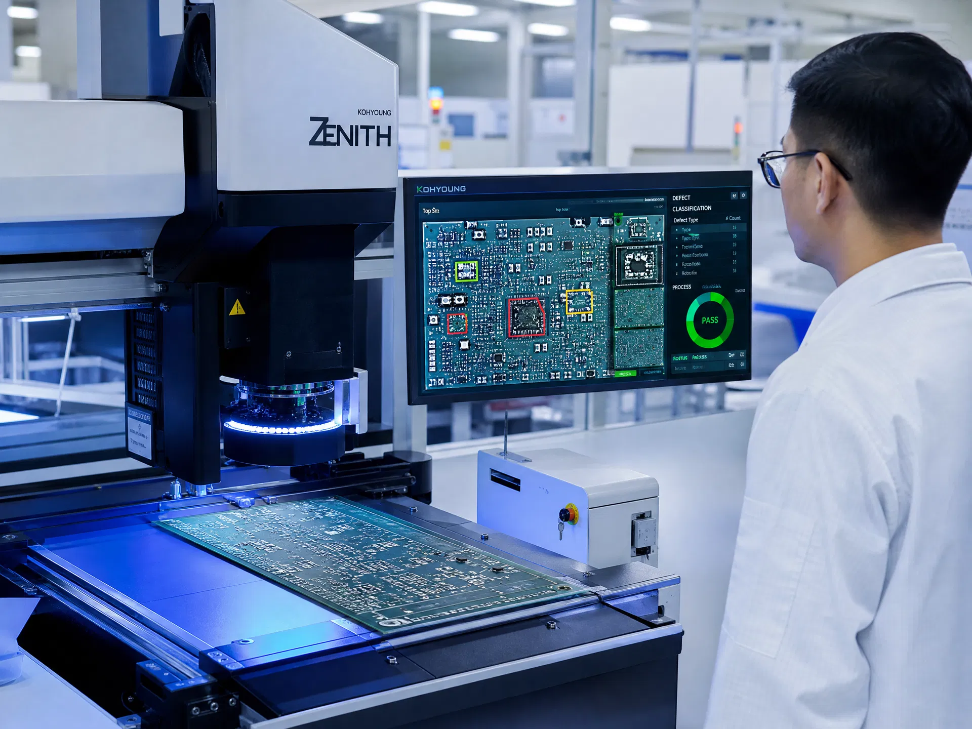
Our placement accuracy of ±0.03mm ensures reliable assembly even for the most demanding high-density designs. The SMT process follows a rigorous sequence: solder paste printing with SPI (Solder Paste Inspection) verification, high-speed component placement, reflow soldering in a nitrogen-atmosphere oven, and 100% AOI inspection after reflow.
For BGA, CSP, and other hidden solder joint packages, X-Ray inspection is available as standard or on-request. Our engineers review every new design for SMT-specific DFM issues — pad geometry, stencil aperture design, component clearances, and thermal relief — before production begins.
Key Capabilities
- 7 Yamaha high-speed SMT placement lines
- Min component: 01005 (0.4 × 0.2 mm)
- Placement accuracy: ±0.03 mm
- SPI (Solder Paste Inspection) after printing
- 100% AOI inspection post-reflow
- X-Ray inspection for BGA and hidden joints
- Lead-free (RoHS) and leaded solder options
- Nitrogen reflow atmosphere available
Service Parameters
| SMT Lines | 7 Yamaha high-speed lines |
| Min Component Size | 01005 (0.4 × 0.2 mm) |
| Min Pitch (QFP/QFN) | 0.25 mm |
| Placement Accuracy | ±0.03 mm |
| Daily Capacity | 10 million placements/day |
| BGA Support | Yes — X-Ray inspection included |
| Solder Paste Inspection | 100% SPI after printing |
| Post-Reflow Inspection | 100% AOI |
| Solder Process | Lead-free (SAC305) / Leaded (Sn63Pb37) |
| Reflow Atmosphere | Air / Nitrogen (on request) |
How It Works
A transparent, step-by-step process designed to eliminate surprises and deliver consistent results.
Stencil Preparation
Laser-cut stainless steel stencil manufactured to your Gerber aperture data. Stencil thickness optimized per component mix.
Solder Paste Printing
Automated paste printing with immediate SPI verification. Any print defects are corrected before placement.
Component Placement
Yamaha high-speed placement at ±0.03mm accuracy. Vision system verifies component orientation and polarity.
Reflow Soldering
Multi-zone reflow oven with profiled temperature curve per solder paste specification. Nitrogen atmosphere available.
AOI Inspection
100% automated optical inspection after reflow. All defects logged and boards reworked before proceeding.
X-Ray & Final QC
X-Ray inspection for BGA and hidden joints. Final visual inspection to IPC-A-610 Class 2 or 3 standard.
Frequently Asked Questions
Explore Related Services
High-Speed SMT for a 5G CPE Antenna Module — 0.3mm Pitch QFN at Scale
A Taiwanese telecom equipment company manufacturing a 5G CPE antenna module — requiring 2,000 units/month with 0.3mm pitch QFN components and strict RF performance requirements.
The Problem
The customer's previous SMT supplier was achieving only 94% first-pass yield on the 0.3mm pitch QFN RF front-end IC, requiring rework on 6% of boards. At 2,000 units/month, this meant 120 boards per month going through rework — adding cost and introducing reliability risk from thermal stress during rework.
Key Challenges
- 0.3mm pitch QFN RF front-end IC — requires precise stencil aperture design and paste volume control
- RF performance sensitive to solder joint quality — voids in QFN thermal pad affect heat dissipation and RF ground
- 2,000 units/month volume — rework cost was significant
- IPC Class 2 workmanship with X-ray verification of QFN thermal pad void percentage
- Nitrogen reflow required for the RF front-end IC per component manufacturer recommendation
Our Solution
We redesigned the stencil aperture for the QFN thermal pad using a 5-segment aperture pattern (instead of the customer's original solid aperture) to achieve the target 50-70% paste coverage that minimizes voids while ensuring adequate solder volume. We set up a dedicated nitrogen reflow profile for this board using our Heller 1950EXL oven with nitrogen atmosphere. 100% X-ray inspection was implemented to measure thermal pad void percentage, with boards exceeding 25% void area flagged for rework. We also implemented SPI (Solder Paste Inspection) after printing to catch paste volume deviations before placement.
Results & Outcomes
"The stencil aperture redesign Kingdta proposed solved our QFN void problem immediately. Moving from 94% to 99.1% first-pass yield on a 2,000-unit monthly run is a significant quality and cost improvement. Their X-ray data gives us the process visibility we need for our RF performance guarantee to our customers."
Quality Manager, Telecom Equipment Company — Hsinchu, Taiwan