
Manufacturing Capabilities & Specifications
Detailed technical specifications for our SMT, DIP, PCB fabrication, and quality testing capabilities.
SMT Assembly Capabilities
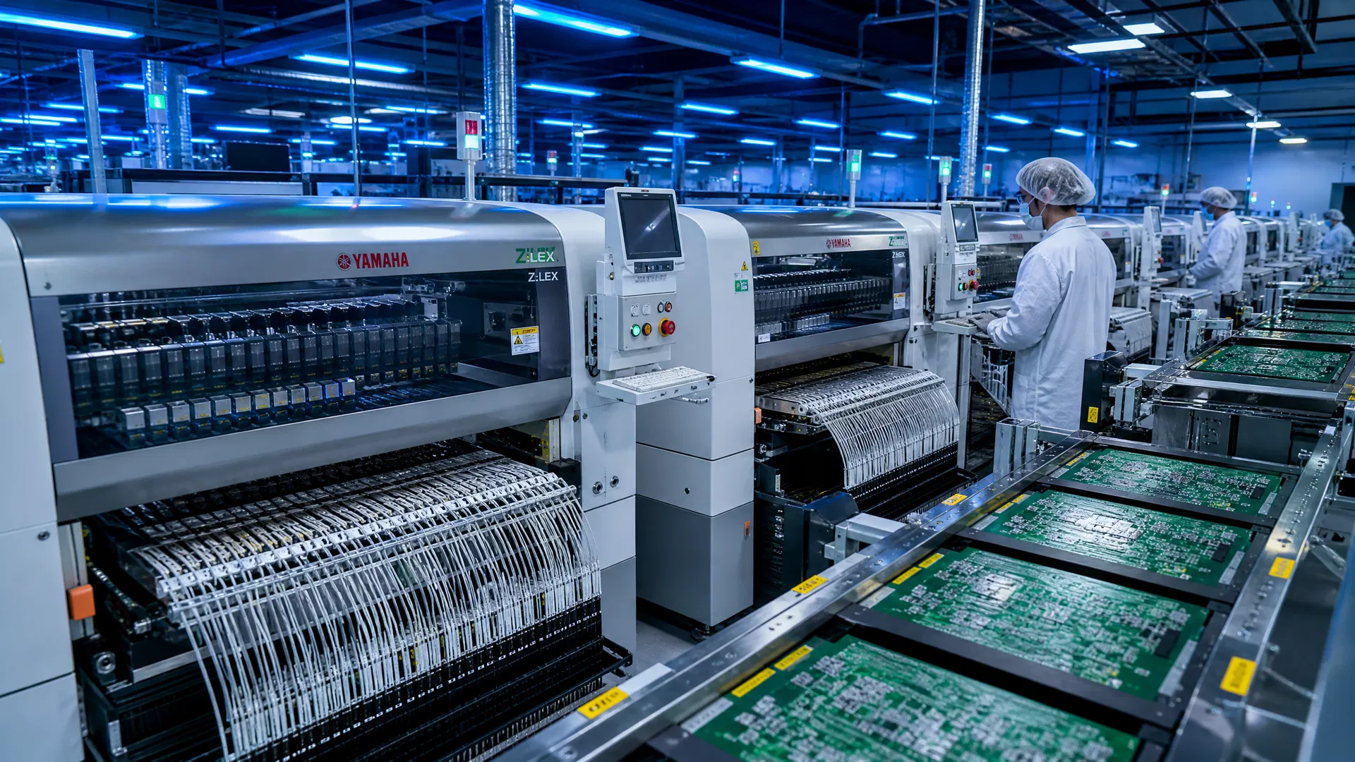
Kingdta operates 7 Yamaha high-speed SMT placement lines with a combined capacity of 10 million component placements per day. Our equipment handles everything from 01005 passives to large BGAs and connectors, with placement accuracy of ±0.03mm.
SMT Specifications
| SMT Lines | 7 Yamaha high-speed lines |
| Daily Placement Capacity | 5,000,000 components/day |
| Placement Accuracy | ±0.03mm |
| Min Component Size | 0201 (0.6 × 0.3mm) |
| Min BGA Ball Pitch | 0.3mm (BGA) / 0.35mm (WLCSP) |
| Component Types | BGA, WLCSP, QFN, POP, Connectors, Wire/Cable |
| Assembly Type | Single/Double-sided SMT, Shield Can Assembly |
| Max Component Height | 25mm |
| Max Board Size | 510 × 340mm |
| Min Board Size | 50 × 40mm (smaller with panelization) |
| Component Packaging | Reel, Cut Tape, Tube, Tray, Loose (post-solder) |
| Solder Process | Lead-free Reflow / Lead-free Wave / Manual Soldering |
| Stencil | Laser-cut stainless steel stencil |
| Inspection | 100% AOI + X-Ray + Manual Sampling |
| Quality Standard | IPC Class 2 |
| MOQ | No minimum — 1 piece accepted |
| Lead Time | As fast as 24 hours |
DIP Assembly Capabilities
Three dedicated DIP lines with wave and selective soldering. Full mixed SMT+THT assembly capability.
| DIP Lines | 3 dedicated plug-in lines |
| Soldering Method | Wave / Selective / Manual |
| Min Lead Pitch | 1.27mm (0.05") |
| Mixed Assembly | SMT + THT on same board |
| Selective Soldering | Available for complex mixed boards |
| Cleaning | Water-wash / No-clean flux |
PCB Fabrication Capabilities
In-house PCB fabrication for 1–20 layer boards. All standard and advanced surface finishes available.
| Layer Count | 2 – 30 layers |
| Board Material | FR-4 (Grade A Jiantao/Guoji), Aluminum (Halogen-free) |
| Max Board Size | 680 × 1200mm (2-layer); 680 × 640mm (4-8 layer) |
| Board Thickness | 0.4 – 2.0mm (0.4/0.6/0.8/1.0/1.2/1.6/2.0mm standard) |
| Thickness Tolerance (>1.0mm) | ±10% |
| Thickness Tolerance (<1.0mm) | ±0.1mm |
| Min Trace/Space | 4/4 mil (0.1/0.1mm) |
| Min Via Drill | 0.2mm |
| Min Via Inner/Outer Diameter | 0.2mm / 0.45mm (multi-layer) |
| Drill Hole Tolerance | ±0.075mm |
| Outer Layer Copper | 1 OZ (35μm) / 2 OZ (70μm) / 3 OZ (105μm) |
| Finished Hole Size | 0.25 – 6.5mm |
| Outline Dimension Tolerance | ±0.15mm |
| Min Trace-to-Edge Clearance | ≥0.3mm (12mil) |
| Solder Mask Colors | Green / Red / Blue / White / Black / Purple |
| Min Silkscreen Width | ≥0.15mm |
| Min Silkscreen Height | ≥0.8mm |
| Surface Finish | HASL, ENIG, OSP, Immersion Ag, Immersion Sn |
| Half-Hole (Castellated) | Up to 10 holes, min diameter 1.0mm |
Testing & Inspection Capabilities
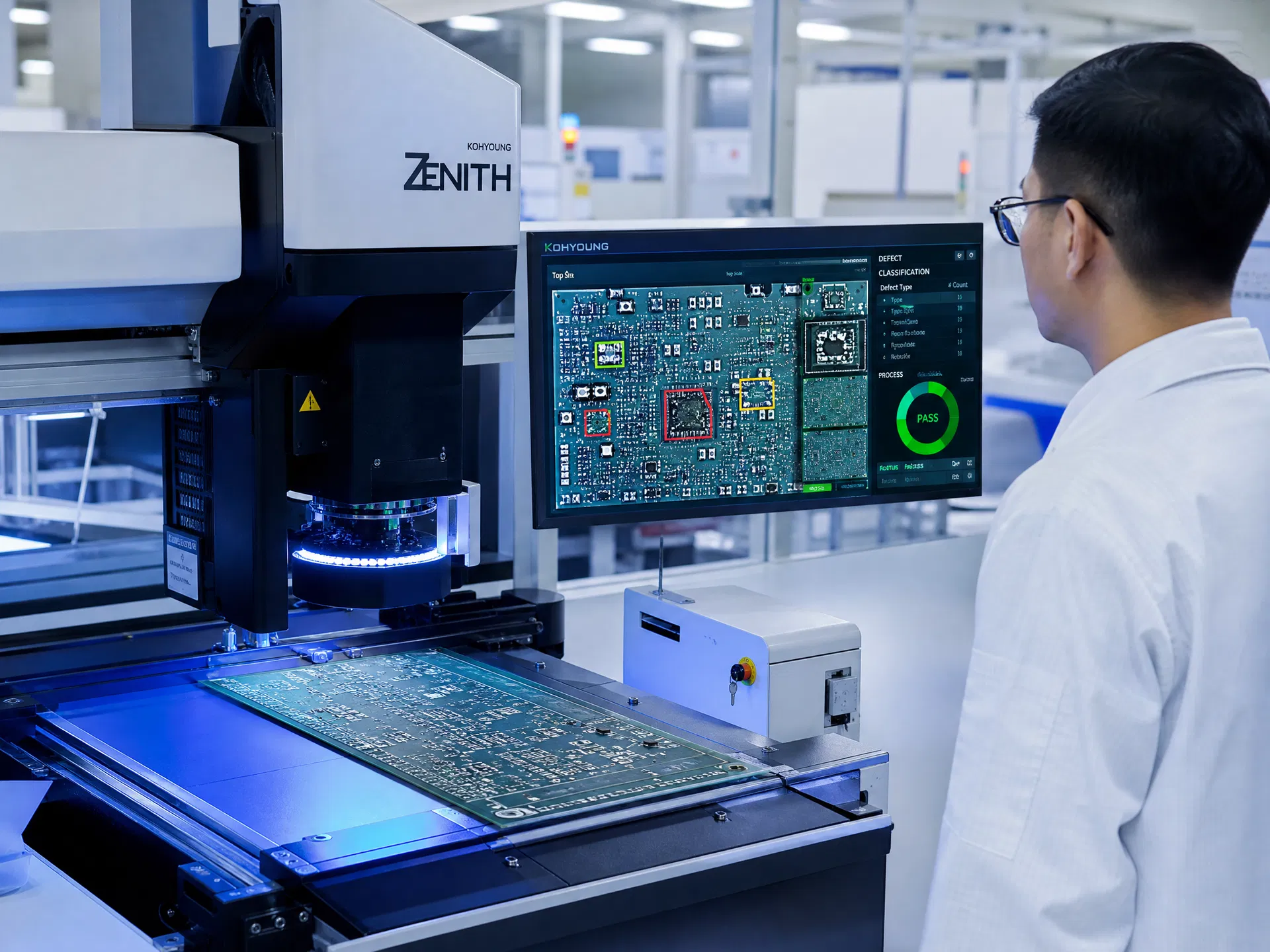
Every board undergoes a multi-stage inspection process. 100% AOI is standard on all orders. X-Ray, ICT, and functional testing are available to meet your specific quality requirements.
Testing Specifications
| SPI (Solder Paste Inspection) | 100% — post-print |
| AOI (Automated Optical Inspection) | 100% — post-reflow |
| X-Ray Inspection | BGA and hidden joints |
| ICT (In-Circuit Test) | Available per customer fixture |
| Functional Testing | Per customer test specification |
| Flying Probe Test | Available for bare boards |
| Burn-in Testing | Available on request |
9-Stage Quality Control Process
Every production order follows this documented quality process. All steps are recorded in our MES system for full traceability.
Pre-Production Engineering Review
Gerber, BOM, and CPL files reviewed by engineers. DFM issues flagged before production.
Incoming Material Inspection
All components verified: resistance/capacitance values, silk screen, PAD matching, pin oxidation check.
First Article Inspection (FAI)
First assembled board verified against BOM using automated first-article tester before full run.
SPI — Solder Paste Inspection
100% automated solder paste inspection after printing. Volume, area, and height verified.
In-Process Monitoring
Placement accuracy and component orientation verified during production. Real-time SPC monitoring.
Reflow Profiling
Thermal profiling for each new product. Profile validated against component and solder paste specs.
AOI — Automated Optical Inspection
100% AOI after reflow. Component presence, polarity, value, and solder joint quality checked.
X-Ray & Functional Testing
X-Ray for BGA and hidden joints. ICT and functional testing per customer specification.
Final QC & Shipment
Visual inspection, anti-static packaging, MES-tracked shipment with full documentation.